This file type includes high resolution graphics and schematics when applicable.
Direct-sampling pipeline analog-to-digital converters (ADCs) produce a large collection of mixing products, much like passive RF/microwave mixers. In high-speed ADCs, these mixing products are sum-and-difference image signal components that extend to microwave frequencies. They are the result of transient signal events—glitches that result from the abrupt connection of sample capacitors when the ADC resumes tracking.
In addition, disturbances conducted into the input network immediately prior to sampling must not be returned during the sampling process. The higher the sampling speed and the greater the resolving power of these ADCs, the more apparent the effects of poor control over these commutation products become—henceforth referred to as “these products.” By paying attention to signal-integrity concerns for these high-speed ADCs, however, it’s possible to limit the damage from these unwanted mixing products.
Simple sum-and-difference products would fold back onto the frequencies at which they appear with the baseband frequency range, and with the exception of some gain error, would disappear. However, unavoidable nonlinear products accompany these simple mixing products and, unless dissipated or absorbed, will result in distortion. A time element is involved, so distance and settling behavior have roles to play in minimizing such distortion.
Issues of Absorption
RF/microwave engineers faced with the task of controlling similar mixing products in a passive mixer will recognize the need for an absorptive network on both the RF and intermediate-frequency (IF) paths, if not on the local-oscillator (LO) path. Engineers may not immediately recognize that they’re dealing with these same issues in an ADC. Once aware of this similarity, an experienced RF engineer is better prepared to deal with the issues. But, the degree of absorption can still be a surprise. The notion of settling behavior is often understood by analog and signal-integrity (SI) engineers. However, it may not be common knowledge that a network exhibiting complete absorption over the broad range of frequencies doesn’t necessarily mean it will exhibit good settling characteristics.
Take, for example, the 210-Msample/s, 16-b LTC2107 ADC from Linear Technology Corp., which has a 80-dB signal-to-noise ratio (SNR). For optimum performance, the VSWR of the analog input path must be very good out through microwave frequencies—the frequency range where these mixing products eventually roll off significantly. This point often goes unrecognized as being a noteworthy concern extending past 5 GHz in modern high-speed ADCs. These mixing products, which are images of the input signal mirrored around every harmonic of the clock source, don’t even start to roll off until beyond 2 GHz. The high SNR of the LTC2107 ADC is a double-edged sword in that the larger sample capacitors employed in this digitizer increase the power in these mixing products, and unfortunately, enhance the capability to resolve the effects of reflections returned from impedance discontinuities.
Absorptive filters have proven to produce good results with these ADCs, but their layout complexity and cost can be daunting. The component count of an absorptive bandpass filter is at least two to three times that of a reflective bandpass of the same order. Even greater complexity may result from measures needed to control the effects of self-resonant frequency (SRF) in final inductors.
Lower-frequency applications can be addressed by using a high-speed feedback amplifier, such as the LTC6409 differential amplifier/ADC driver from Linear Technology. Its source port is terminated, with its low output impedance padded to produce correct source termination, but followed with a lumped-element differential diplexer for performing the task of mixing-signal absorption at higher frequencies. As such, this functions as an absorptive source for the high-speed ADC. Simple series source termination fails to produce good return loss (in terms of S22 performance) above a certain frequency as amplifier output impedance rises upward.
At microwave (GHz) frequencies, it can be challenging to achieve adequate return loss for fully absorptive inductive-capacitive (LC) filters, such as bandpass filters (BPFs) or lowpass filters (LPFs), due to limitations imposed by the SRFs of inductors, inductance of capacitors, effects of short transmission-line segments between elements, and the more obvious parasitic pad capacitance under the elements. To address these issues, Soshin Electric Japan developed a low-temperature-cofired-ceramic (LTCC) differential diplexer (model HMD6117J-T) for Linear Technology that presents a simple, compact way of answering the shortcomings of various input networks.
The LTC6430 high-linearity, differential RF/IF amplifier/ADC driver is a wideband differential gain block, matched to 50 ⦠(100 ⦠in differential hookups). However, above about 500 MHz, its return loss is inadequate for the needs of the LTC2107 ADC. At 1 GHz, the output return loss is about 10 dB, whereas the ADC requires better than 20-dB return loss to achieve its full spurious-free dynamic range (SFDR). A 10-dB return loss at 1 GHz and above can produce more than a 20-dB compromise in SFDR.
Implement a Differential Diplexer
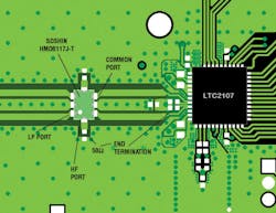
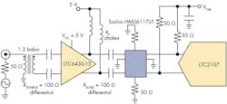
Soshin’s HMD6117J-T differential diplexer handles the mixing products for frequencies above 400 to 500 MHz, and presents an absorptive character extending to 3 GHz and beyond to the ADC. In the process, it diverts the higher-frequency mixing products into a pair of termination resistors placed on the high-band ports. In doing so, it also reduces the high-frequency disturbances and mixing products seen by the amplifier. Used in conjunction with the LTC6430 differential gain-block amplifier/ADC driver (Fig. 1), the combination produces a compact inexpensive driver solution, suitable for frequencies extending from about 20 to 400 MHz. Anti-aliasing should be performed prior to the amplifier for frequency-domain applications.
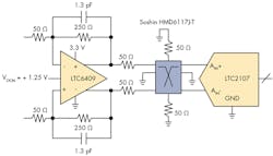
When used with the LTC6409 driver, the HMD6117J-T differential diplexer provides a complete solution for applications from dc to 100 MHz (Fig. 2). For time-domain applications that have essentially flat spectral power distribution, with no risk of strong interferers above about 100 MHz, this topology may be used to 200 MHz—or beyond 200 MHz if the spectral power distribution rolls off with frequency.
The differential diplexer can be used in a similar manner with the LTC6417, a unity-gain differential buffer amplifier, and possibly with other feedback amplifiers. For applications requiring as much SNR as possible, the HMD6117J-T differential diplexer can also be used after an absorptive bandpass filter to improve return loss at high frequency, which simplifies the filter, makes the layout less critical, simplifies the choice of inductors, and reduces the number of required high-quality RF termination resistors.
The diplexer may also be used following a transmission-line balun to improve an input network’s high-frequency behavior, as well as reduce the noise bandwidth of an RF gain block (Fig. 3). The LTC2107 digitizer and a number of other direct-sampling ADCs do not perform well if driven by a transmission-line transformer in close proximity to the ADC. If the transmission-line transformer is placed more than 6 in. from the LTC2107, performance may be sufficient, but the additional space required on a printed-circuit board (PCB) may not be acceptable.
Other Key Benefits
The adverse effects of many transmission-line transformers are in part due to asymmetry in the construction of the Guanella balun, unequal line lengths, time skew between the lines in the twisted pair running through the binocular core, and undesired coupling between successive passes through the core. These factors can produce return reflections as well as asymmetry in the returned products. Common-mode transients translated to differential form by asymmetrical returns will degrade SFDR. The diplexer will hide this asymmetry from the ADC, allowing use of a single-ended absorptive filter or a single-ended drive amplifier prior to a balun, and enabling these to be closer to the ADC.
The diplexer might provide a greater degree of freedom for using flux-coupled transformers that have poor impedance balance above 400 MHz. Transformers with extended low-frequency response often have too much interwinding capacitance to perform well with high-speed ADCs. Other thin-film baluns that do not behave well at high sample rates may be aided by the diplexer, too. Note that the diplexer does not act as a balun. Drive signals must be amplitude- and phase-balanced in the passband, as well as being at least nominally absorptive in the region below 500 MHz.
Use of the diplexer may be advisable if the ADC’s drive signals originate on the other side of a PCB, where it may prevent the complexity of the transmission path through the vias from coming into play, or compensate for generally poor impedance control of PCB traces. Producing a 50- ⦠transmission line through a viahole requires a large relief around the viahole, as well as a significant collection of viaholes defining the barrel for conducting ground current. The internal layers must not have annular rings at each copper layer, and should have a minimal ring at the surface. In any case, the abrupt change of direction at the surface produces a pair of impedance discontinuities; in a thick PCB, these are not close enough to each other to cancel. All of the traces between the driver and ADC should be “controlled impedance” 50- ⦠lines. The 50- ⦠terminators may be some distance away if those traces are well-controlled 50-⦠lines. Poor impedance control requires that they be close to the diplexer.
The pair of 50-⦠resistors on the highpass ports required should be 1% edge-trimmed high-frequency resistors or terminators, rather than 0.1% precision trimmed resistors, which can be poor at high frequency. The diplexer measures 3.2 × 2.5 mm.
This file type includes high resolution graphics and schematics when applicable.
Achieving full performance in high-speed, direct-sampling ADCs requires attention to signal integrity in all ports involved in the devices, which means essentially every pin. The analog input is simply the most demanding, followed closely by the clock. The differential LTCC diplexer developed by Soshin Electric and Linear Technology largely resolves issues with reflections in the analog-input paths, be these from impedance discontinuities, poorly controlled trace impedance, layer changes, connectors, less than optimal return loss (S22) at high frequency from amplifiers and transformers, and low SRF of inductors. Use of this device may mitigate RFI issues and provide other benefits beyond the scope of this article.
Derek Redmayne is a staff scientist at Linear Technology Corp.


