Bandpass Filter Passes 2.4- and 5.2-GHz Bands
This file type includes high resolution graphics and schematics when applicable.
As communications systems have spread, dual-band filters have become essential components in RF front-end modules for sorting and screening signals in different frequency bands. A great deal of research has been conducted on different methods for realizing such filters.1-5 For example, in one approach,2 two homocentric microstrip perturbed ring resonators were fabricated on the same layer to obtain dual-mode dual-band filter responses. The resonators were fed by coplanar waveguide (CPW), resulting in a wide range of external quality factors (Qs).
In another approach,3 two homocentric embedded defected ground waveguide (DGW) resonators were adopted for a dual-band filter design, each fed by a 50-Ω microstrip line. In another work,4,5 a dual-band bandpass filter with meander-loop resonator and complementary split-ring resonator defected ground structure (SRR DGS) was proposed. Finally, an aperture compensation technique was proposed for enhancing the coupling in the parallel-coupled microstrip lines employed in these filters,6 although there is yet little research available on combining dual-band filter designs with the aperture compensation technique.
For improved performance in dual-band communications applications, a dual-band bandpass filter (BPF) was developed. It features a dual-mode resonator and SRR DGS excited with common improved input/output (I/O) coupling structure using an aperture compensation technique. The improved I/O structure is designed to provide greater coupling than traditional coupling structures without adding size. The performance of the improved coupling structure was confirmed by means of two-port equivalent-circuit analysis. The coupling structure and filter achieves high selectivity by the use of several finite attenuation poles within the stopbands.
This new design approach also offers a great deal of flexibility in the manner of independently controllable center frequencies within the passbands and bandwidths that can be tuned over a wide range. The filter structure is relatively simple and compact. The design approach was applied to the development of a dual-band filter for use at the wireless-local-area-network (WLAN) frequency bands of 2.4 and 5.2 GHz.
This file type includes high resolution graphics and schematics when applicable.
A New Approach
This file type includes high resolution graphics and schematics when applicable.
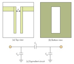
The new filter approach includes an improved I/O structure that employs an aperture compensation technique. Figure 1(a) shows a traditional I/O coupling structure with complete ground plane, while Fig. 1(b) offers the improved coupling structure with defected ground plane. Both structures can be equivalent to the structure shown in Fig. 1(c). Equation 1 details the transfer function of the two-port network:
H(s) = (1/sCp2)/[1/sCs + 1/ sCsp1] = Cs /(Csp2 + Cs) (1)
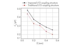
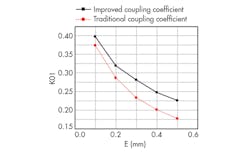
where it can be seen that the amplitude of H(s) is proportional to capacitance Cs. As the amplitude of H(s) is increased, the energy transferred between the two ports is increased, which means that the coupling coefficient is also increased. The value of Cs changes according to the change of distance e (Fig. 2). Figure 2 indicates that an improved structure can provide greater coupling than conventional coupling structures. As evidence of this, Fig. 3 provides simulated results of an improved input/output (I/O) coupling coefficient in comparison with a traditional I/O coupling coefficient. As can be seen from Fig. 3, it is possible to achieve stronger coupling with an improved structure in the same physical size as a conventional coupling structure.
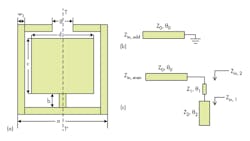
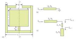
The improved dual-mode resonator structure is shown in Fig. 4(a). The dual-mode characteristics are realized by loading a stepped-impedance-line stub at the center of the open-loop resonator. Since the resonator is symmetrical to the T-T' plane, the odd- and even-mode method can be applied to analyze it. The equivalent circuit of Fig. 4(b) can be applied for analysis of the odd-mode excitation. The one-port input impedance of that equivalent circuit can be found with the aid of Eq. 2:
Zin,odd = jZ0tanθ0 (2)
From the resonant condition that Yin,odd = 0, the first odd-mode resonant frequency can be determined by means of Eq. 3:
fodd = c/[4(2a – g/2)(εeff)0.5)] (3)
where:
c = the speed of light in free space, and
εeff = the effective dielectric constant of the substrate material.
For an even-mode excitation, the equivalent circuit of Fig. 4(c) should be applied. Its one-port input impedance can be found by means of Eqs. 4-6:
Zin1 = -j(1/ Z2tanθ2) (4)
Zin2 = Z1[(Zin1 + jZ1tanθ1)/(Z1 + jZin1tanθ1)] (5)
Zin, even = Z0[(Zin2 + jZ0tanθ0)/( Z0 + jZin2tanθ0)] (6)
From the resonance condition that Zin,even = 0, it is possible to achieve the equality of Eq. 7:
R1R2tanθ0tanθ1tanθ2 - R1tanθ0 – tanθ1 - R2tanθ2 = 0 (7)
where:
R1 = Z1/Z0, and R2 = Z1Z2.
Under the special condition that Z0 = Z1 = Z2, the first resonant frequency can be found by applying Eq. 8:
feven = c/[2(2a – g/2 + b + c)(εeff)0.5] (8)
Equations 3 and 8 show that changing the values of b and c only affects the even-mode resonant frequency, leaving the odd-mode resonant frequency unchanged. Knowing this, by adjusting the values of b and c, the even-mode resonant frequency can be tuned while also adjusting the center frequencies and bandwidths.
This file type includes high resolution graphics and schematics when applicable.
A Closer Look
This file type includes high resolution graphics and schematics when applicable.
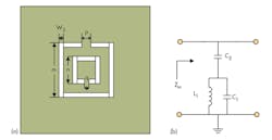
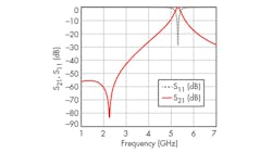
Figure 6(a) shows the topology of the SRR DGS. From an equivalent circuit of the SRR DGS7 shown in Fig. 6(b), it is possible to find the location of the transmission zero for the SRR DGS cell according to the desired resonant frequency of the shunt circuit. This resonant frequency can be found by means of Eq. 9:
fs = 1/2π[L1(C1 + C2)]0.5] (9)
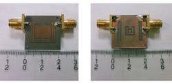
Figure 9 is a photograph of the fabricated dual-band filter. Simulations and measurements were accomplished by means of the High Frequency Structure Simulation (HFSS 13.0) simulation software and model E5071C microwave vector network analyzer (VNA), respectively, both from Agilent Technologies (now Keysight Technologies).
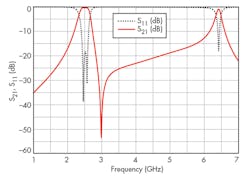
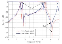
Figure 10 presents simulated and measured results for the proposed filter. The two filter passbands are centered at 2.53 and 5.11 GHz, with minimum insertion losses of 1.1 and 3.0 dB, respectively, for the two passbands. The return losses within the two passbands were better than 14 dB. Two attenuation poles were realized for the dual-band BPF structure, at 2.83 and 6.08 GHz, which helped to greatly improve the selectivity of the proposed dual-band BPF. As can be seen from the plots, the measured results mainly agree with the simulated performance values. Discrepancies between the measured and simulated performance levels (Fig. 8) can be attributed to fabrication tolerances in realizing the dual-band filter on commercial microwave circuit substrate material.
Wu Guo-An, Professor
Zhang Bi-Xia, Master’s Degree Candidate
Xu Qin-Fen, Lecturer
Li Wen-Guang, Lecturer
Institute of Microwave Technology Application, Huazhong University of Science and Technology, Wuhan, 430074, People’s Republic of China
This file type includes high resolution graphics and schematics when applicable.
References
This file type includes high resolution graphics and schematics when applicable.
1. Jin Xu, Wen Wu, and Chen Miao, “Compact and Sharp Skirts Microstrip Dual-Mode Dual-Band Bandpass Filter Using a Single Quadruple-Mode Resonator (QMR),” IEEE Transactions on Microwave Theory & Techniques, Vol. 61, No. 3, March 2013, pp. 1104-1113.
2. Xiu Yin Zhang and Quan Xue, “Novel Dual-Mode Dual-Band Filters Using Coplanar-Waveguide-Fed Ring Resonators,” IEEE Transactions on Microwave Theory & Techniques, Vol. 55, No. 10, October 2007, pp. 2183-2190.
3. H.W. Liu, L. Shen, Z.C. Zhang, J.S. Lim, and D. Ahn, “Dual-Mode Dual-Band Bandpass Filter Using Defected Ground Waveguide,” Electronics Letters, Vol. 46, 2010, pp. 895-897.
4. G.-L. Wu, W. Mu, X.-W. Dai, and Y.-C. Jiao, “Design of Novel Dual-Band Bandpass Filter with Microstrip Meander-Loop Resonator and CSRR DGS,” Progress in Electromagnetic Research, Vol. 78, 2008, pp. 17-24.
5. Jahyeon Lee and Yeongseog Lim, “A Dual-Band Bandpass Filter Using Capacitively I/O Coupling,” Microwave & Optical Technology Letters, Vol. 55, 2013, pp.1823-1825.
6. Lei Zhu, Huizheng Bu, and Ke Wu, “Aperture Compensation Technique For Innovative Design Of Ultra-Broadband Microstrip Bandpass Filter,” in IEEE MTT-S International Microwave Symposium Digest, 2000, pp.315-318.
7. B. Wu, B. Li, T. Su, and C.-H. Liang, Equivalent-Circuit Analysis and Lowpass Filter Design of Split-Ring Resonator DGS, Journal of Electromagnetic Waves and Applications, Vol. 20, 2006, pp. 1943-1953.
This file type includes high resolution graphics and schematics when applicable.
