CMOS Models Transistor Distortion
Nonlinear behavior in active devices can lead to distortion and lost information in communications systems that rely on those devices. Because silicon CMOS transistors are so widely used in analog, digital, and mixed-signal circuits, understanding the nonlinear characteristics of these transistors can serve to improve performance in highly integrated circuits (ICs). To that end, a new transistor model was developed for high-frequency silicon CMOS transistors, using a superposition method to quantify the individual contributions of different nonlinear elements.
The model is implemented entirely using symbolically defined devices (SDDs) to represent each nonlinear parameter. The real-life basis for the model is a 0.18-μm RF silicon CMOS foundry device capable of operation to 10 GHz. With the help of the Advanced Design System (ADS) suite of simulation software tools from Agilent Technologies (www.agilent.com), the SDD model will be validated by examining the behavior of the table-based model against a foundry transistor modeled in a single-tone sweep test—from extremely small signals to input levels large enough to cause transistor compression.
Silicon CMOS is a versatile semiconductor technology, useful for both analog and digital functions. Its low-power operation has placed it at the heart of many portable wireless devices. It is a common semiconductor building material for mixed-signal devices, including data converters and gate arrays. As silicon CMOS foundries improve their capabilities, CMOS transistors continue to rise in frequency and power levels, now commonly reaching frequencies well into the microwave range. This provides legitimate competition for more exotic III-V compound-semiconductor devices, including GaAs high-electron-mobility-transistor (HEMT) devices1 and traditional silicon bipolar transistors. Yet CMOS devices are often overlooked in terms of characterization and model development, especially at higher RF and microwave frequencies where they are being increasingly used.
As communications systems move toward higher-level modulation formats in an attempt to transfer data at increasingly high rates, the linearity of these systems becomes a prime concern. This holds true not only for large-signal amplifiers, but also smaller-signal transceivers and their components. Even low-noise amplifiers (LNAs) must provide linear operation, particularly at low bias levels, in order to preserve the overall linear performance of
the transceiver.2
A silicon CMOS transistor has a number of sources that can contribute to distortion, including the device transconductance, gm, nonlinear device capacitances (such as the gate-source capacitance, Cgs and the drain-source capacitance, Cds), and the output conductance, gds. Many previous studies have examined CMOS transistor linearity,3-5 but most of this research studied the distortion of the device as a whole using mathematical representations. To the best of the current authors’ knowledge, accurate quantifications of individual distortion sources—either within silicon CMOS or GaAs transistors—has never been attempted in this manner. Some attempts have been made to model transistor nonlinear behavior where some of the individual nonlinear contributions were combined at a high level, for example, in ref. 6.
However, it is the authors’ belief that in order to truly understand the nonlinear behavior of a silicon CMOS transistor, it must be treated as a collection of nonlinear contributions—one where each nonlinear parameter is independent of the others. The contribution of each nonlinear element to the total distortion of the transistor can be quantified by using a superposition approach. This superposition method as proposed here is unique in that it maintains the individual distortion contributions as completely independent of each other. The superposition method proposed here involves switching between linear and nonlinear representations of nonlinear parameters in the model, one at a time. To facilitate this, the transistor must be modeled in a way which represents every nonlinear element individually and independently from other nonlinear elements.
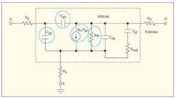
This nonlinear modeling exercise is based on a 0.18-μm RF silicon CMOS transistor from a commercial foundry design kit. One advantage of using a foundry design kit transistor is that it facilitates a more robust verification of the model via testing the transistor model and comparing simulated and measured results. Figure 1 shows the small-signal model used to represent the silicon CMOS transistor. The parameters inside and outside the dashed square are the intrinsic and the extrinsic parameters, respectively. The nonlinear behaviors of the circled parameters will be modelled and quantified.
1. This small-signal transistor model is the basis for the nonlinear silicon CMOS
transistor model. It is based on a foundry device capable of operation to 10 GHz.
Resistance Rg is the effective lumped gate resistance of the transistor, consisting of both the electrode resistance and the distributed channel resistance. Resistances Rs and Rd represent the effective source and drain resistances of the device, consisting of the via, salicide, contact, and LDD resistances. Capacitances Cgs and Cgd are the effective gate-to-source and gate-to-drain capacitances of the CMOS transistor, and consist of both the intrinsic and overlap capacitances of the transistor.
Parameter Csd is the source-to-drain capacitance of the transistor. This nonlinear model does not include the transcapacitance, Cgd − Cdg, since tests on the model show that this parameter has little impact on the accuracy of the device Y-parameters (Y12 and Y21), as suggested by ref. 7. Parameters gm and gds represent the device transconductance and the output conductance of the transistor, respectively. Capacitance Cjd consists of both the drain-junction capacitance and the intrinsic drain-to-body capacitance, while resistance Rsub is the drain-to-substrate resistance of the device.
To extract values for these parameters, a modified version of the method presented in ref. 7 was used. The modification is related to the deembedding of the extrinsic components to produce expressions for calculating the intrinsic components. In ref. 7, that author refers to ref. 8 and suggests that only the gate resistance, Rg, is to be deembedded from the Z-parameters measured at a desired operating bias condition. This is because, owing to the terminal source and drain resistances, the poles are at a much higher frequency than the typical transit frequency. Hence, they can be neglected when calculating the Y-parameters of the equivalent circuit.
But tests performed by the current researchers show also that not deembedding source resistance Rs and drain resistance Rd will lead to a significant variation in the resulting forward transmission characteristics, S21, between the new model and the previously modelled transistor parameters. To verify the accuracy of the modification, an S-parameter sweep simulation from 1 to 10 GHz was carried out. Results show a good match between the magnitudes and phases of the S-parameters of the new CMOS model and the existing foundry model for the CMOS transistor. These results are not shown here due to space limitations.
It should be noted that the CMOS transistor’s transconductance and the output conductance, gm and gds, exhibit partially nondispersive behavior. Figure 2 shows the extracted values of gm and gds over the range of the transistor’s operating frequencies. It is clear that the values of gm and gds do not change significantly between low and high frequencies, especially to 2 GHz. This somewhat validates that gm and gds can be represented as two nonlinear independent current sources in the saturation region.
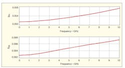
2. As part of building a nonlinear model, the values of the CMOS transistor’s transconductance and output conductance, gm and gds, respectively, were extracted across the device’s expected operating frequency range.
To build a table-based nonlinear model using SDDs, values for the essential device parameters were required at different bias points. To avoid repeating this process over the complete operating range of the transistor, a sweep simulation was created for the bias range of interest. A structure was then built to employ the indexing feature within ADS’ Data Display Window, so as to sample data generated for the different independent parameters. The results were then analyzed as part of the evaluation of the remaining, dependent device parameters. Using this structure, it was possible to plot the variance of each nonlinear element with respect to the change in bias conditions.
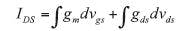
The silicon CMOS transistor’s transconductance and output conductance were modeled separately using two separate table-based current sources. Because of the partially nondispersive nature of the transistor, the DC current contribution due to gm and gds can be effectively split, without the need of integration, by using this equation:
The separate current contributions from these nonlinear elements were extracted at DC from the transistor’s DC characteristic curves. To make the current split, the authors used a complex structure of indices in the ADS simulation program to identify the point at each Vgs curve at which Vds − Vgs + VT = 0 is satisfied. That is the transition, or "knee" point, at which the transistor switches from triode to saturation regions of operation. A horizontal Ids line was then plotted from this point. The current contribution from the gate-source transconductance, gds, was calculated to be the difference between actual transistor current (variant with Vds due to gds) and the horizontal (not varying with Vds) current assumed if the effect of gds was neglected. This process was repeated for every Vgs curve.
Figure 3 shows how the current was split. In Fig. 3(a), a horizontal line was plotted from the knee of the chosen Vgs curve. Figures 3(b) and 3(c)show the currents that are produced as a result. In Fig. 3(c), the gate-drain-source current, Idgs, remains at zero until the knee starts increasing. In Fig. 3(b), the transconductance current (Igm) varies normally with the gate-source voltage (Vgs) and the drain-source voltage (Vds) until reaching the knee and then becomes constant. It should be noted that this approach of splitting the current is only valid in the device’s saturation region; as a result, only the results of this saturation-current split were used for the model. In the device’s triode region, Vds actually influences Igds so that Ids should not be zero in that region and Igm should not be equal to Ids. The current split was performed in this way to allow the currents to be added and the DC characteristics of the transistor to be reconstructed. By operating the transistor in the saturation region, the results of the current split should be valid.
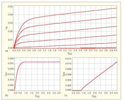
3. The device DC current was split in terms of transconductance and output conductance currents, Igm and Igds, respectively.
Using the values of the nonlinear parameters produced from the automated extraction structure, the SDD model—which comprises seven table-based SDD components for all the model parameters—was constructed. The produced values of the nonlinear parameters at the respective gate and drain voltages were placed in a software table which is accessed by the SDD representing each parameter. The performance between the measured points was interpolated to ensure a correct description of harmonics and convergence within harmonic balance (HB) simulations.
Figures 4 (a), (b), and (c)show how the current source, a resistance, and a capacitance were modeled respectively. In Fig. 4(a), the capacitor current, Ic is modeled using the simple differential equation, Ic = C dVc/dt, where the 1 in the output current, (I[3,1]) represents a differentiation which is predefined in the SDD. Contrary to ref. 9, the authors found that modeling the capacitor as a charge-conservative element rather than by its direct current does not have a huge impact on the magnitudes of the produced harmonics.
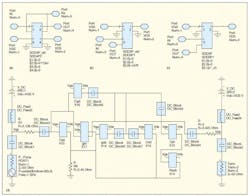
4. These diagrams show a nonlinear SDD for (a) a capacitor, (b) a resistor, and (c) current, along with a top view (d) of the model constructed by adding the partial currents.
The voltages of ports 1 and 2 (which are mapped to Vgs and Vds) are linked through a data access component in ADS to the table which contains values for capacitance subject to Vgs and Vds. In a similar manner, a resistor’s current was modeled as shown in Fig. 4(b)using Ohm’s law and dividing the resistor’s voltage by the value sourced from the software table. In Fig. 4(c), a current source was modeled directly by equating the current at the output port to the current stored in the software table.
In Fig. 4(d), the whole model is constructed in a manner comparable to the small-signal model of Fig. 1. For the model to be truly nonlinear, values of parameters in the model should be variable subject to the DC bias, as well as to the input power superimposed on the DC level at each bias point. Therefore, the controlling voltages at ports 1 and 2 of each SDD (upon which values from the interpolated table would be passed to the SDD and used), are connected to the mixed (DC + RF power) input of the circuit not above or below the DC feed or the DC blocking components. In this way, the value selected from the table will depend on the DC bias and the input power, allowing the model to better represent more nonlinear events.
To verify the accuracy of the nonlinear silicon CMOS transistor model, a single-tone harmonic-balance test was conducted with the input power swept from −10 to +18 dBm. This input power range made it possible to focus on the area of the device characteristics where the transistor is in compression. Figure 5plots the fundamental-frequency and third-harmonic outputs from the model across the sweep range of input values for both the newly modeled transistor and the existing transistor foundry model. As can be seen from the curves of Fig. 5, the new model’s output matches the output of the existing transistor model to a great extent. This means its nonlinear behavior—and hence, its nonlinear representation—is highly accurate.
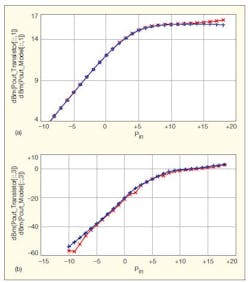
5. These plots show the results for a single-tone harmonic-balance analysis, with output power in both graphs plotted as a function of input power.
The authors believe the SDD-based model is the first table-based transistor model to represent each of the nonlinear distortion contributions individually in such a detailed manner. This is useful when, during the development of new devices at the foundry, as an example, it is necessary to examine model and device parameters separately during device optimization and/or refinement. This modeling approach has also provided quantification of the contribution each of these elements adds to the total distortion of the device. The quantification superposition method relies on the total portability of the model. Quantification works by replacing the SDD representing the nonlinear parameter under test by a linear component, with the actual value at the bias point at which the transistor is operating. In this case, the magnitude of the third harmonic (in dBm) at an input level of 0 dBm was used to make comparisons between the distortion levels when the device parameters are represented in either linear or nonlinear fashion. These results are still being finalized at press time, and will be reported in a forthcoming article.
In summary, a nonlinear, table-based model has been developed for a silicon CMOS transistor, building upon the available knowledge of that transistor’s behavior from its foundry process. This model has been validated by comparing its results to those of a linear model under various bias and input-power conditions. The new model helps quantify the contribution of each nonlinear element in the transistor to the total distortion of the device, achieved by switching the representation of the model elements between linear and nonlinear elements. Such a model is invaluable in better understanding the nonlinear mechanisms of this silicon CMOS transistor and in projecting its performance under different operating conditions. Further improvements to this model remain to be made in increasing the bias and input power ranges at which the model is accurate and converges in a harmonic-balance simulation.MWRF
Acknowledgment
Ali Abuelma’atti would like to thank the Institute for System Level Integration in Livingston/Scotland for their financial support of this work.
References
1. W. Guo and D. Huang, "The noise and linearity optimization for a 1.9-GHz CMOS low noise amplifier," Proceedings of the IEEE Asia-Pacific Conference on ASIC, 2002, pp. 253-257.
2. T.W. Kim, B. Kim, I. Nam, B. Ko, and K. Lee, "A low power highly linear cascoded multiple-gated transistor CMOS RF amplifier with 10 dB IP3 improvement (revised)," IEEE Microwave and Wireless Components Letters, Vol. 13, 2003, pp. 420-422.
3. P. Park, C.S. Kim, and H.K. Yu, "Linearity, noise optimization for two stage RF CMOS LNA," Proceedings of IEEE Region 10 International Conference on Electrical and Electronic Technology, TENCON 2001, 2001, Vol. 2, pp. 756-758.
4. I. Kwon and K. Lee, "An integrated low power highly linear 2.4-GHz CMOS receiver front-end based on current amplification and mixing," IEEE Microwave and Wireless Components Letters, Vol. 15, 2005, pp. 36-38.
5. V. Aparin, G. Brown, and L.E. Larson, "Linearization of CMOS LNA’s via optimum gate biasing," Proceedings of the IEEE International Symposium on Circuits and Systems, ISCAS’04, 2004, Vol. 4, pp. IV-748/IV-751.
6. I. Schmale, "An improved physics-based nonquasi-static FET model," Proceedings of the 27th European Microwave Conference and Exhibition, 1997, pp. 328-333.
7. A.F. Tong, K.S. Yeo, L. Jia, C.Q. Geng, J.-G. Ma, and M.A. Do, "Simple and accurate extraction methodology for RF MOSFET valid up to 20 GHz," IEE Proceedings: Circuits, Devices and Systems, Vol. 151, 2004, pp. 587-592.
8. C. Enz and Y.H. Cheng, "MOS transistor modeling for RF IC design," IEEE Journal of Solid-State Circuits, Vol. 35, 2000, pp. 186-201.
9. Z. Heshmati, I. C. Hunter, and R.D. Pollard, "MMIC frequency dividers," First Electromagnetic Remote Sensing Defence Technology Centre Technical Conference, Edinburgh, 2004, paper No. C9.
ALI ABUELMA’ATTI, Doctor, Department of Electronics & Electrical Engineering, University of Glasgow, Glasgow, Scotland, United Kingdom, e-mail: [email protected]
IAIN THAYNE, Professor, Department of Electronics & Electrical Engineering, University of Glasgow, Glasgow, Scotland, United Kingdom
MUHAMMAD TAHER ABUELMA’ATTI, Professor, King Fahd University of Petroleum and Minerals, Dhahran 31261, Saudi Arabia, e-mail: [email protected]
