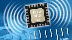
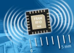
Like all members of the FerVID family, the MB89R112 series employs ferroelectric random-access memory (FRAM). FRAM is touted for providing fast write speeds, high-frequency re-writing, and a good level of radiation tolerance—all while being conservative in terms of power consumption. With 9 kB of FRAM, the company claims that its product provides the greatest density available in an RFID chip operating in the high-frequency (HF) band as defined in ISO/IEC 15693 (see photo).
With 9 kB of FRAM, this device claims to offer the highest density available in an RFID chip operating in the HF band (as defined in ISO/IEC 15693).
A total of 8 kB of this capacity is provided as user memory, enabling access by read/write operations as defined in ISO/IEC 15693. The series will be offered in two variants with 24- and 96-pF input capacitance. Writing 8 kB of data takes about 4 s, which is 6X faster than the time it takes E2PROM products.
With these memory devices, the increased available data volume on RFID tags would enable greater operating characteristics in applications like product-lifecycle traceability management and equipment maintenance records. According to Fujitsu, these memory devices can provide solutions spanning embedded, industrial, and medical applications.
What Engineers Want
For engineers, the higher-capacity memory—combined with the RFID connectivity to sensors and microcontrollers—can enable the wireless modification of product operating parameters or the logging of environmental factors during distribution. These features would benefit production control in automotive and electronics manufacturing. They also would aid maintenance applications in aviation, construction, and civil engineering.
The MB89R112QN products enable these features by supplementing the HF RFID interface with an additional Serial Peripheral Interface (SPI) for microcontroller connectivity. Because the 8 kB of user memory in FRAM can be accessed from the microcontroller via SPI, shared memory regions can be used both for data logging and as a parametric area for changing the microcontroller’s operating parameters.
Development Backstory
For eight years, Fujitsu has been developing FRAM products as part of the FerVID family. The firm uses two frequency bands for the chips integrated in high-functionality RFID tags operating in the HF band from 3 to 30 MHz. Also known as the decameter band or decameter wave [as the wavelengths range from one to ten decameters (10 to 100 m)], Fujitsu’s designs operate at 13.56 MHz and an ultra-high-frequency (UHF) band covering 860 to 960 MHz. As a result, these products serve a wide range of chips including those used in data-carrier tags in factory automation and maintenance, those that can withstand gamma radiation or electron beams for the medical and pharmaceutical sectors, and chips with serial interfaces for embedded applications.
What is FRAM?
Ferroelectric random-access memory (FRAM) is a nonvolatile form of memory that uses ferroelectric film as a capacitor. Possessing characteristics of both read-only-memory (ROM) and RAM devices, FRAM features high-speed access, high endurance in write mode, low power consumption, and nonvolatility. It also is very tamper-resistant. Consequently, it is used in smart cards and mobile phones, where high security and low power consumption are critical.
Ferroelectric thin films with a perovskite crystalline structure are suitable for a range of applications, such as nonvolatile memories, dynamic random-access memories (DRAMs), solid-state displays, infrared detectors, pyroelectric and piezoelectric sensors, and microwave devices. Thus, PZT [Pb (ZrTi)O3] material is widely used as a ferroelectric material. When it is subjected to an electric field, the Zr/Ti atom shifts up or down. This polarization remains when the electric field is removed, providing nonvolatility while keeping power consumption low.


