Simulate A Doherty Amplifier With DPD
This file type includes high resolution graphics and schematics.
Doherty amplifiers can deliver power with high efficiency and excellent linearity over a wide dynamic range. A Doherty amplifier comprises carrier and peaking amplifiers linked by a quarter-wave transmission line. The carrier amplifier is typically biased for linear operation—for example, Class A or AB—while the peaking amplifier is typically biased for nonlinear operation (e.g., Class C). As input power is increased, the peaking amplifier gradually turns on, thereby augmenting the power being produced by the carrier amplifier. When properly designed, the total power of the amplifier is increased, with better linear performance and efficiency.
The use of digital predistortion (DPD) for improved linearity is gaining popularity as power amplifier designers seek high efficiency and reduced adjacent-channel power ratio (ACPR). To demonstrate the design of a Doherty amplifier, we show a typical design with the aid of Microwave Office® circuit design software from AWR Corp. A critical aspect of the design is to correctly account for the various nonlinearities in the transistors.
The amplifier will be designed and constructed based on transistor technology from NXP Semiconductors. The operating points and optimal loads for the amplifier will be determined using standard load-pull techniques. Electromagnetic (EM) simulation will be used to model critical sections of the amplifier layout, where low-impedance output matching sections are so broadband that closed-form models tend to be inaccurate. In particular, the output section will be simulated by means of the planar EM simulator AXIEM® from AWR. Although the main circuit simulator used for modeling the Doherty amplifier is harmonic-balance software, a number of other simulation options will be discussed—including the use of circuit-envelope simulation.
A Doherty amplifier can provide high power-added efficiency (PAE) for applications where power is critical, such as in cellular base stations. The Doherty amplifier was originally invented in 1936 by William H. Doherty of Bell Telephone Laboratories. Details of the design have changed through the years—including its migration from vacuum tubes to transistors as the active devices—but the basic concept remains intact. Doherty amplifiers have become increasingly popular in recent years because of their capability to handle large peak-to-average signals, as are typified in wireless applications.
Figure 1 shows a generic Doherty amplifier topology. It essentially features two amplifiers in parallel. The top amplifier is biased under Class AB conditions, while the bottom amplifier is powered as a Class C unit. The Class AB amplifier is designed to operate as a linear amplifier, thereby giving very low distortion. Unfortunately, it is not very efficient, with maximum theoretical efficiency being about 78.5%.
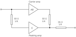
1. This simple block diagram shows the topology of a Doherty amplifier. Class AB and Class C amplifiers are used in parallel for improved power efficiency.
Note that a Class AB amplifier is more efficient than a Class A version because two transistors are used in parallel and are biased such that each is on 50% of the time. Class B bias is the limiting case of Class AB bias conditions. Under Class AB conditions, the bias is set to have the regions where the transistors are turned on overlap slightly. This minimizes the problem of crossover distortion, which is a degradation of performance caused by the nonzero voltage drop required for turning on the transistors.
The Class C amplifier is used as the peaking amplifier in the circuit. A Class C amplifier is biased so that the transistor only turns on when there is non-zero input power above a predetermined threshold level coming into it. This makes for a very efficient amplifier, but one that is highly nonlinear. The idea of the Doherty amplifier is to use the Class AB amplifier at low power. At higher power the Class C amplifier also contributes to the output power. Hopefully, this leads to increased PAE at higher power levels. Note that the circuit contains two quarter wavelength matching sections at the frequency of operation. These sections are necessary as the input impedances of the amplifiers are changing, and it is critical that the entire circuit be well matched over all power levels.
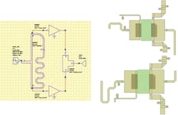
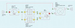
The Doherty amplifier described in this report is based on transistors from NXP Semiconductors. Figure 2 shows the high-level conceptual schematic circuit and layout for the Doherty amplifier circuit. The various portions of a typical Doherty amplifier can be clearly seen. For example, the layout shows the Class AB (top of Fig. 2) and the Class C (bottom of Fig. 2) amplifiers. The feed lines differ by 90 deg. at the intended point of operation.

2. A top-level schematic of the amplifier is on the left, with the layout of the two amplifiers on the right.
The illustrative Doherty amplifier was designed with the aid of Microwave Office software, using the standard design methodology for this type of circuit. Load-pull simulations were run to determine practical input and output loads—a first step in determining impedance-matching networks. Figure 3 shows a typical load-pull plot.
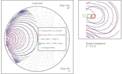
3. These load-pull simulation results show constant output power curves (blue curves) and PAE curves (purple curves). The red circle shows the load point for maximum output power; the green square the load for maximum power efficiency.
The blue curves are constant-output-power curves, as the output load is varied. The purple curves plot the PAE for a given output load. The maximum output power is attained when the (normalized) load is at the location of the red circle. The maximum PAE is attained when the load is at the green square. Fortunately, the square and circle are found at about the same load, from 2 to 2.5 Ω. The output-matching network is shown in Fig. 4.
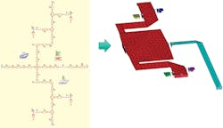
4. The output-matching network was originally designed using transmission line models, as the schematic shows on the left. The resulting layout was simulated using AXIEM, AWR’s planar EM simulator.
The original Doherty amplifier design was created using standard transmission-line models. However, these models are inadequate for the extreme aspect ratios required for the low-impedance-matching network. As the lines become very wide, the accuracy of the models becomes compromised. The layout was therefore simulated in AXIEM, a planar EM simulator well suited for planar layouts.
The meshed EM layout is shown in the right half of Fig. 4. The layout is color-coded to show the DC connectivity of the various shapes. It is important to note that it was not necessary to manually export the amplifier layout to the EM simulator. Rather, AWR’s EM extraction technology was used, which makes it possible to effortlessly send the desired parts of a circuit layout to an EM simulation, where ports were added automatically. The simulated S-parameter results were used in the amplifier schematic circuit instead of the models, resulting in a more accurate solution.
This file type includes high resolution graphics and schematics.
The circuit was then modeled using AWR’s harmonic-balance simulation technology. Figure 5 shows the DC bias lines of the transistors, as well as the dynamic load lines for the Class AB and Class C amplifiers that comprise the Doherty amplifier. The purple curves are the dynamic load lines for the Class AB amplifier, while the green curves are the load lines for the Class C amplifier.
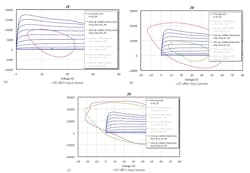
5. These are bias lines and dynamic load lines for the Doherty amplifier’s transistors at different voltages (a, b, and c). The purple curves are for the class AB amplifier. The green curves are for the Class C amplifier. As the input power increases, the Class C amplifier turns on.
As can been seen, the input power increases from +26 dBm to +40 dBm; the Class C amplifier turns on and contributes to the increase in output level. (Note that the load lines include the effects of package parasitics, which is why can have negative voltage and current values.) Figure 6 shows the output power (the blue curve and left axis) and the PAE (the purple curve and right axis) for the completed amplifier. The efficiency increases to about 56%, which is about 7% higher than either the Class AB amplifier or the Class C amplifier alone.
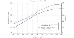
6. These plots show the output power (blue curve and left axis) and the PAE (purple curve and right axis) for the Doherty amplifier.
The performance of the amplifier can be further improved by correcting for various nonlinearities and mismatches in the system. There are several ways to accomplish this. This paper illustrates one method that is particularly useful for modern mobile encoding schemes using digital pre-distortion. The technique increases the range over which the amplifier is linear, thereby reducing distortion. AWR’s Visual System Simulator™ (VSS) software was used to carry out the analysis.
7. This is the amplifier’s correction topology as modeled in VSS. The input power is corrected by the I/Q table values, and then combined to give the corrected results.
VSS uses nonlinear system models for the amplifier to determine the overall system response. The modeling approach is to simulate in-phase/quadrature (I/Q) values with the uncorrected amplifier, then create a correction table within the VSS simulator as shown in Fig. 7. Correction factors are calculated for the various input power levels to create the desired output. The input power is multiplied by the corrected I/Q table values. Once the tables have been calculated, they can be programmed into the amplifier’s control circuitry. They need not be changed unless the operating conditions of the amplifier change, at which point they would need to be recalculated.
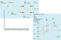
8. This is the complete VSS system, with a fully specification-compliant LTE input signal.
Figure 8 shows the complete system level analysis with a fully specification-compliant test signal; for this evaluation, a Long Term Evolution (LTE) cellular signal was used. Figure 9 shows the improvement in the amplifier’s performance, illustrated by three channels in the spectrum. The corrected signal (red curve) features a reduced noise floor when compared to the uncorrected system (blue curve). Figure 10 shows the corrected AM-AM and AM-PM curves. Noticeable improvement can be seen: The corrected amplifier has 3-dB increased output power and the AM-PM distortion has been nearly eliminated.
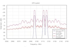
9. The Doherty amplifier’s input channels are shown by the blue curves. The uncorrected (purple curve) and corrected (red curve) results are shown. The noise floor has been lowered by 20 dB.
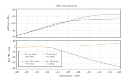
10. These plots show the AM-AM and AM-PM measurements for the uncorrected and corrected amplifiers. The phase distortion is improved 30 deg. by the correction, while the output power is increased 3 dB.
This example has thus far used harmonic-balance modeling as the circuit simulation methodology; however, AWR offers a second approach to simulating the circuit—namely, circuit-envelope simulation. While straightforward and efficient, harmonic balance does have its shortcomings. In particular, it cannot model memory effects, and only simulates steady-state performance. The system simulations carried out in VSS in this example used nonlinear behavioral models, based on the AM-AM and AM-PM characteristics of the amplifier. It did not take into account memory effects or circuit level issues such as currents in the biasing network.
Envelope simulation, on the other hand, is a circuit-level simulation method that takes longer to simulate than harmonic balance, but allows for memory effects. Figure 11 shows an example of the type of results possible (in this case using a PA manufactured by Infineon). The red (nonlinear behavior) and green (envelope simulation) curves differ slightly. The slight shift in frequency is typical of memory effects.
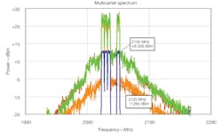
11. This plot shows the spectrum of a multicarrier system.
The orange curve is the DPD-corrected amplifier, with clear improvement being shown in the results. The input signal is in blue, a conventional nonlinear behavioral model is shown in red, the envelope simulation isdepicted in green, and the DPD circuit is shown in orange. Since envelope simulation is a circuit-based simulator, it can also show the time-varying currents and voltages at various points in the circuit. For example, Fig. 12 shows the DC and RF drain currents under modulated signal conditions.
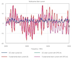
12. These plots show the amplifier’s DC and RF drain currents under modulated signal conditions.
In summary, the use of a commercial circuit simulator such as AWR’s Microwave Office can simplify the design of a DPD-based Doherty amplifier, especially when EM simulation is used as part of the modeling process. In addition, a DPD network was created in VSS software, yielding performance improvements (Figs. 9 and 10). As was presented, a number of different simulation methods are available for designing such an amplifier—that said, different programs account for different operating conditions and effects, and simulation times may vary.
Editor’s Note: More information on circuit envelope simulation is available in the four-page PDF white paper, “Leverage Circuit Envelope Simulation to Improve 4G PA Performance,” available for free download.
Mark Saffian, Solution Architect
John Dunn, EM Technologist
AWR Corp., 1960 E. Grand Ave., Ste. 430, El Segundo, CA 90245; (310) 726-3000, FAX: (310) 726-3005, e-mail: [email protected], www.awrcorp.com.
This file type includes high resolution graphics and schematics.
