RF Materials Can Open The Gates For Next-Generation Technology
This file type includes high resolution graphics and schematics when applicable.
RF/microwave technology is finding a home in new fields every year and even creating industries and areas of study. The miniaturization and increased cost efficiency of modern RF/microwave technology allows for wireless enhancement to almost any technological application. Communications electronics, medical sensing/monitoring, and state-of-the-art aircraft are just a few of the fields that are heavily influenced by these enhancements. With the rapidly increasing use of wireless technology, the market is being pushed to develop more advanced materials and methods. In fact, a few categories of materials in particular are creating a buzz around the potential benefits of next-generation wireless technologies.
Related Articles
• Perusing Materials For High-Frequency PCBs
• Benefit From High-Dk Microwave Circuit Materials
• Materials Support High-Speed Circuits
The first cutting-edge category on the list is a group of conductors that exceed even the highest conductivity potential of copper, silver, or gold. These “superconductors” differ fundamentally from conventional materials in the manner by which electrons move through the material on a quantum level. Such quantum behavioral differences lead to unique properties like zero resistance conduction, high current density, high sensitivity to magnetic fields, and near speed-of-light signal transmission. As noted by Oleg Mukhanov, senior vice president and general manager for Government Operations at HYPRES, Inc., "Superconductivity provides a number of performance advantages, critical for many applications from RF systems, medical systems, to high-end computing."

When it comes to advancing wireless technologies, superconductors allow for the near-lossless transmission of high-frequency signals with very low external interference. This benefit has huge real-world impact—especially within the telecommunications industry. The division of cellular telephone signals into small channels using modern filters reduces the range and quality of cellular communication. The dissipation of signal energy through imperfect filters and signal processing causes this degradation. In doing so, it leads to a significant cost increase as telecommunications companies require higher-power signal towers or more towers in a network for adequate coverage.
Additionally, imperfect filters require wider bandwidth for each channel, thereby reducing the number of simultaneous connections. Superconductor filters provide near-lossless current flow, perfect diamagnetism, and lack of dispersion, which could increase the number of channels for a standard telecommunications setup while reducing the minimum required strength of the signals for processing.
With superconductor-enhanced analog-to-digital converters (ADCs), the speed of wireless communications could be enhanced many fold, according to a white paper by HYPRES titled "Benefits of Superconductor Digital-RF Transceiver Technology To Future Wireless Systems." Superconductors provide linearity, quantum accuracy, and near-light-speed transmission intrinsically. This enhancement could completely expunge the need for the digital signal to be analog preprocessed before it is converted into a high-frequency signal, allowing direct digital-to-high-frequency conversion.
With superconductor digital microelectronic circuits operating at speeds near 100 GHz, the frequency and protocol-specific analog hardware in wireless systems can potentially be replaced with flexible, software-programmable digital processors. These benefits could lead to a completely software-defined radio (SDR) that could behave as a universal system, where the hardware could be adapted to almost any platform. Lower receiver noise temperatures would enhance information capacity--even where interference normally limits full-bandwidth utilization. Transmitters also would benefit from being able to generate spectrally pure waveforms with completely linear amplifier chains. The U.S. Government and many commercial ventures are already leading the development of superconductor technologies for wireless communications.
Such enhancements would also impact the sensing, instrumentation, and radar fields, where superconductors enable the most sensitive detection of electromagnetic (EM) radiation. In addition, the instrumentation field benefits from the extreme magnetic-field sensing capability of superconductor circuits, which can be seen in instruments designed from superconducting quantum interface devices (SQUIDS). From detecting indicators of potential oil fields and salt domes from the air to chemistry, physics, and material-science laboratories, such instruments will continue to allow for cutting-edge advancements. SQUID detectors also are used as the most sensitive EM detectors of space-born signals and are used in several radio observatories around the world. Additionally, the high dynamic range of superconducting digitizers allows for the detection and identification of sea-skimming missiles for anti-ship missile-defense radar.
Many companies, like HYPRES, are already developing high-speed computers and advanced wireless-communications systems using superconducting technologies. Superconductor Technologies, Inc. (STI) offers several low-noise receiver front ends, duplexers, and antenna multiplexers that use cryogenic superconducting technology. Though superconductors offer potentially huge benefits for the RF/microwave fields, presently there are only a limited number of applications in which the modern superconductor can be used. Cryogenic cooling is needed to ensure proper superconductivity, which is not possible in all applications. As the uses for superconductor technology increase, the need to raise the operating temperature of superconductors has increased as well. Future superconductors could range in size from nanometer connections between transistors all the way to ultra-low-loss, high-power cable lines.
This file type includes high resolution graphics and schematics when applicable.
Metamaterial Prospects
This file type includes high resolution graphics and schematics when applicable.
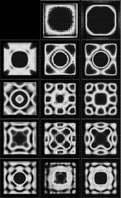
A less developed but equally promising category of new materials is metamaterials. There are many definitions for exactly what a metamaterial is, but the root understanding is that metamaterials are man-made structures that exceed the capability of natural materials. This area could be exciting for microwave engineers, as the periodic array of sub-wavelength structures that make up a metamaterial exhibit EM responses that are not typically found in nature (Fig. 4). Among the potential results could be magnetic metamaterials with very low loss, magnetic materials with very low dispersion, negative permeability structures, negative permittivity structures, artificial impedance surfaces, and a host of other potentially beneficial effects that are ideal for future sensing and communication systems. Generally, the capabilities of these new materials could lead to size reductions, lower costs, and higher speeds--all high-demand benefits of the microwave industry.

Some examples of metamaterial applications include frequency-selective surfaces (FSSs), compact multiband antennas, EM bandgap structures, resonant permittivity/conductivity sensors, precise hyperthermia tools, and strain sensors. An example of the unique EM behavior of several metamaterial arrays is shown in Fig. 3.
Raytheon is already working with several universities and industry partners to develop practical uses for these materials . Raytheon’s goal is to add capability while reducing the size of its EM products using metamaterial technology. For example, high-performance aircraft have less available real estate for wireless technology as the capabilities and performance of the aircraft increase. This reduction leads to the need for broader bandwidth, dual polarization, and wide-angle scanning capability from multi-function conformal-antenna structures. Current structures suffer from narrow scan angles and bandwidths, but metamaterial antenna enhancements could prove the deciding factor in realizing the high end requirements. In a collaboration with the University of Florida, Raytheon is developing reduced-size, dual-band, metamaterial Global Positioning System (GPS) antennas. Current technologies are limited by the narrowband function that is a feature of many resonant metamaterials. But this collaboration’s goal is to enhance the multiband capability of the GPS antennas.
Electronic bandgap structures are made by using periodically placed grounded vias. In higher-dielectric-constant substrates, their use can result in an increase in the bandwidth and scan-angle performance of the microstrip patch antenna arrays that require such substrates. Through the use of metamaterial techniques like electronic bandgap structures, the surface waves that limit the scan-angle performance can be disrupted, thereby enhancing performance.
Metamaterials also are being heavily explored by the scientific community for their size reduction and unique sensing capabilities for medical applications. Currently, research efforts are being directed to solutions like a highly efficient dual-band antenna operating at the universal mobile telecommunication system (UMTS) band and the industrial, scientific, and medical (ISM) band. Efforts also are being directed toward developing microwave devices that could detect cancer cells with low cost and high precision. Because cancer cells have significantly different water content than normal tissue, they also have higher permittivity and conductivity. With a suitably sensitive biosensor array with metamaterial resonators, these diseased tissues could be precisely identified with a fast and non-invasive detection method. Additionally, high concentrations of microwaves are capable of heating internal tissue. A precise and directed emission of microwaves from a metamaterial lens with a negative-refractive index could be used to focus on a target area and induce hyperthermic death of the tissue.
The unusual resonant behavior of modern metamaterials and future wideband metamaterial structures can offer benefits to RF applications that could not be previously realized, as size and cost were prohibitive. It should be noted that current metamaterials do have a flaw in their narrow bandwidth capability. With adequate research and development advances in metamaterial structures, however, the future could offer highly compact, power-efficient RF structures with spectacular properties. Another category of materials that also offer benefits of size and cost reduction of RF electronics are carbon-based electronic materials.
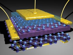
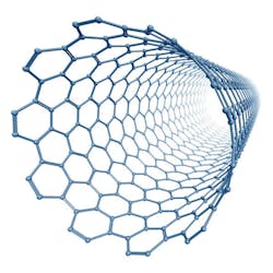
Carbon-based electronics are standard electronic elements that are enhanced with high performing carbon-based materials that have only recently been discovered and successfully fabricated. The two most common carbon-based electronic materials discussed for RF applications are graphene nano-ribbons (GNRs; a monoatomic layer of carbon atoms as seen in Fig. 1) and carbon-nano-tubes (CNTs), a mono-atomic tube of carbon atoms (Fig. 5). These new materials are attracting significant attention from both researchers and engineers because of their extraordinary electrical/optical behavior. With their nanometer dimensions, superior strength, extremely high carrier mobility, semiconductor behavior, and predictions of up to terahertz performance, many experts consider GNRs and CNTs to be the next revolution in high-speed computer fabrication and RF electronics.
It is important to understand the similarities and differences between GNRs and CNTs in regard to their material properties and potential benefits for specific applications. CNTs exhibit one-dimensional (1D) carrier transport. This channeled electron motion reduces the scattering probability by directly increasing the current carrying capacity. It also lowers the thermal noise profile while increasing the size of the mean free path through the CNT. Models that predict terahertz performance have been derived from applications like employing CNTs as channels in a field-effect transistor (FET). The high carrier velocity of up to 80 million cm/s and very low quantum capacitance allow for a very fast-recovering, highly linear, and near-ballistic transport-based CNTFET. Such characteristics are ideal for future ultra-high-speed RF amplifiers, mixers, and switches.
GNRs also have exhibited extremely high mobility that reportedly ranges up to 100 times that of silicon (Si). In addition, they boast ambipolar transport properties, capability for electrostatic doping, and a thin/flexible structure that is a good fit for many RF applications. Among such applications are those with low-noise amplification and high-sensitivity as well as mixers and reconfigurable circuits.
Both carbon-based materials have drawbacks spanning fabrication to negative interface interactions. The atom-thick layer of carbon in GNRs and CNTs causes degradation of bandgap voltage, carrier mobility, Schottky barrier height, and effective charge density when embedded in a transistor structure in close proximity to other materials. There also are many fabrication difficulties to overcome with the creation of suitable carbon-based electronics. Current fabrication techniques degrade the overall performance of the materials while complicating integration into modern fabrication processes. Despite these challenges, companies like RFnano are already producing and working on the next stage of CNT implementations for the RF industry.
Related Articles
• Perusing Materials For High-Frequency PCBs
• Benefit From High-Dk Microwave Circuit Materials
• Materials Support High-Speed Circuits
As for the research debates over which carbon-based material is better for ultra-high-frequency operations with FET devices, experiments with graphene field-effect transistors (GFETs) and CNTFETs have been performed by many labs. GFETs tend to have high output conductance, which lowers the internal voltage gain to a factor much lower than 1. This prevents GFETs from operating as high-gain circuits. CNTFETs have voltage gains slightly larger than 1. For example, a discrete amplifier built by MITEQ using CNTFETs fabricated by RFNano was detailed in the study, "L-band carbon nanotube transistor amplifier." This amplifier allegedly exhibited 11-dB power gain at 1.3 GHz and 6 dB power gain at 2 GHz. In a recent study by IBM, "Ultimate RF Performance Potential of Carbon Electronics," both the power-gain and current-gain cutoff frequencies of CNTFETs and GFETs were found to exceed 1 THz. Those cutoff frequencies are much higher than silicon-nanowire or gallium-arsenide (GaAs) semiconductors. It was also found that CNTFETs require lower biasing currents, are less sensitive to fabrication defects, and have higher cutoff frequencies than GFETs.
In closing, the technology for fabricating carbon-based electronics is still several years away from being incorporated into mainstream electronics. Given the promising experimental results of high-performing carbon materials, however, the semiconductor roadmap looks solid—even after the RF industry’s demands exceed the limits of Si or GaAs.
This file type includes high resolution graphics and schematics when applicable.
Sources
This file type includes high resolution graphics and schematics when applicable.
"Benefits of Superconductor Digital-RF Transceiver Technology To Future Wireless Systems."
"L-band Carbon Nanotube Transistor Amplifier," IEEE Electronics Letters, Feb. 2011, p. 265.
"Ultimate RF Performance Potential of Carbon Electronics," IEEE Transactions on Microwave Theory & Techniques, Oct. 2011, p. 2739.
"Realizing the Potential of Metamaterials."
"An Overview of Metamaterials in Biomedical Applications," PIERS Proceedings, March 2013.
About the Author
Jean-Jacques DeLisle
Jean-Jacques graduated from the Rochester Institute of Technology, where he completed his Master of Science in Electrical Engineering. In his studies, Jean-Jacques focused on Control Systems Design, Mixed-Signal IC Design, and RF Design. His research focus was in smart-sensor platform design for RF connector applications for the telecommunications industry. During his research, Jean-Jacques developed a passion for the field of RF/microwaves and expanded his knowledge by doing R&D for the telecommunications industry.
