Materials Form Foundations for RF/Microwave Circuits

This file type includes high resolution graphics and schematics when applicable.
Materials pave the way for high-speed, high-frequency circuits. Whether those materials form the packages, the substrates, the printed-circuit boards (PCB), or even the thermal pathways for dissipating heat, they are essential to electronic circuits ranging from DC to optical wavelengths.
PCB materials are starting points for many designs, and an understanding of the key characteristics of these materials can benefit almost any RF/microwave circuit design. Relative dielectric constant (referred to as “relative” for its value in reference to a vacuum), for example, will determine the dimensions of transmission-line structures, such as microstrip and stripline transmission lines at a desired impedance.
Another critical PCB material characteristic is coefficient of thermal expansion (CTE), which is a measure of how a material expands with changing temperature. Ideally, the value should be as close as possible in the X and Y (length and width) directions of the material as the conductive layer, typically copper (16.7 ppm/°C). In doing so, the dielectric material and the copper circuit traces expand and contract with temperature at the same rate, and a minimal amount of dislocations occur in the interface between the two materials (which would result in performance degradation and reliability problems). In addition, by exhibiting low Z-axis (through the thickness) CTE, plated-through-holes in a PCB will also remain stable with temperature.
Circuit materials for RF/microwave applications are available from a wide range of quality suppliers, including Arlon, Isola, Panasonic PCB materials, Rogers Corp., and Taconic. All offer a variety of materials in a number of sheet sizes, with different dielectric constants.
Some, in fact, are developing environmentally friendly versions of PCB materials, such as RO4835HF halogen-free PCB materials from Rogers Corp. and Green Speed materials from Isola, which can be processed in the manner of low-cost FR4 circuit materials.
An area of interest for PCB materials is for millimeter-wave-frequency (above 30 GHz) applications, expected to grow with increased use of millimeter-wave circuits in automotive and Fifth-Generation (5G) wireless systems. Such applications, such as automotive radar systems at 77 GHz, will require PCB materials with low relative dielectric constants and low loss, and high consistence across the material to minimize frequency and phase variations for those small wavelengths at 77 GHz.
For those circuit designs that require special assistance from a substrate material, materials known as metamaterials have been engineered for specific applications. These are materials that can be refined for specific uses—e.g., for miniature antennas or resonators/oscillators—by engineering particular characteristics in a material or a combination of materials. For example, these electromagnetic-bandgap (EBG) materials can be used to increase the gain and bandwidth of a microstrip patch antenna while at the same time reducing its volume.
In fact, the U.S. Air Force is currently seeking research papers in pursuit of metamaterials for enhanced microwave and optical performance. The agency has invited submissions for funding of research ($750,000 available for the first year) on various technologies related to the development of electromagnetic (EM) metamaterials. This applies for acoustic, optical, and RF/microwave use, including the fabrication of reactive electronic matching networks, frequency-selective structures, and periodic structure with engineered dispersion. The deadline for submissions for 10 possible awards is February 20, 2016.
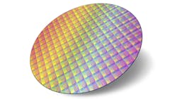
In the semiconductor part of the RF/microwave industry, another set of materials supports the miniature devices and integrated circuits (ICs), including silicon, silicon carbide (SiC), gallium arsenide (GaAs), and gallium nitride (GaN). GaN, with its excellent high-frequency, high-power capabilities, has become one of the more popular semiconductor materials for RF/microwave device developers.
According to a recent report from Research and Markets, “Global GaN Semiconductor Devices Market 2015-2019,” the global GaN semiconductor devices market is expected to grow at a compound annual growth rate (CAGR) of 20.77% in terms of revenue during the period from 2015 to 2019. The report considers GaN semiconductor use in a wide range of markets, including in automotive electronics, consumer electronics, and defense and aerospace applications. Both high-power semiconductors and light-emitting diodes (LEDs) are considered.
GaN is also a favorite substrate material for LEDs, with about one-half of GaN substrates currently being produced around the world being used for blue, green, and white LEDs. To support the strong global demand, China-based material supplier Nanowin recently announced plans to produce 2-in. GaN wafers for blue and green LEDs. The firm forms high-quality GaN films on sapphire substrates using electrodeless photoelectrochemical nanostructure etching techniques and controlled growth conditions. These approaches help relieve stress within the GaN films and produce materials with low defect densities. Another GaN material supplier, Kyma Technologies, has already moved to larger (3- and 4-in. wafers) diameter wafers to keep pace with the growing global demand for the semiconductor material.
Of course, GaAs wafers are still home to a wide range of small-signal discrete devices and ICs for RF/microwave use, and GaAs materials are very much in demand globally. If anything, the strong demand for GaN materials helps with the competitive costs of GaAs substrates. Leading suppliers such as Sumitomo Electric Industries offer semi-insulating GaAs wafers in 100 and 150 mm diameters, with wafers available for epitaxial or ion-implantation applications.
Semiconductor device packaging is also dependent upon advances in materials to meet the cost and performance expectations of emerging markets. For example, most power semiconductors, from audio through microwave frequencies, at one time were housed in expensive ceramic/metal packaging. With time and growing competitive cost concerns, those more-expensive package materials are being replaced by plastic and composite-material packaging which can effectively dissipate the heat produced by high-power devices at all frequencies.
Other materials occasionally used in RF/microwave applications are high-temperature-superconductor (HTS) materials, typically built around yttrium barium copper oxide (YBCO) or niobium materials. Such materials can achieve required temperature levels without a cryocooler and can provide extremely low-loss performance, such as for bandpass filters with negligible passband insertion loss and a fraction of the size of conventional room-temperature filters.
This is just a sampling of the many materials at work within the RF/microwave design community. With the continuing miniaturization of devices for use in wireless systems, and the many sensors expected to feed data to IoT devices, energy management and thermal management become concerns—e.g., keeping things powered and at manageable temperatures. For those purposes, materials for thermal management and power management will become more critical for maintaining high reliability.
In addition, minimizing interference among all those densely placed electronic devices will require proper shielding, and the use of suitable materials for this purpose. But that is a topic for yet another report.
This file type includes high resolution graphics and schematics when applicable.
About the Author
Jack Browne
Technical Contributor
Jack Browne, Technical Contributor, has worked in technical publishing for over 30 years. He managed the content and production of three technical journals while at the American Institute of Physics, including Medical Physics and the Journal of Vacuum Science & Technology. He has been a Publisher and Editor for Penton Media, started the firm’s Wireless Symposium & Exhibition trade show in 1993, and currently serves as Technical Contributor for that company's Microwaves & RF magazine. Browne, who holds a BS in Mathematics from City College of New York and BA degrees in English and Philosophy from Fordham University, is a member of the IEEE.
