Thermal Analysis is Vital for High-Power MMIC, MCM, and RF PCB Apps
Members can download this article in PDF format.
What you’ll learn:
- Why thermal management must expand beyond the PA to the package, PCB, and related circuitry.
- Today’s thermal challenges related to wireless-enabled devices and systems.
- A simulation workflow to perform thermal analysis for RF applications within the design framework.
RF/microwave power amplifiers (PAs) dissipate power, which leads to a rise in operating temperatures that can extend from the single IC stage to an entire, highly integrated RF system. Higher temperatures degrade both the immediate and long-term performance of RF electronics.
Such temperatures are directly linked to reduced device lifetime or mean-time-to-failure (MTTF) for metal semiconductor field-effect transistor (MESFET), pseudomorphic high-electron mobility transistor (pHEMT), and heterojunction bipolar transistor (HBT) devices used in gallium-arsenide/gallium-nitride (GaAs/GaN) monolithic microwave ICs (MMICs). Reliability and MTTF are of special concern for harsh environments and applications that are hard to service, such as remote base stations and satellite communications.
RF designers need to expand their concern for thermal management beyond PAs to include the package, PCB, and surrounding electronics. It’s important to determine the channel temperature for devices based on the large-signal operating conditions, dissipated power, device geometry, and heat-sinking properties of the device and its environment.
For that reason, PA development teams increasingly rely on a mechanical-engineering or thermal-analysis team to investigate operating temperatures either through thermal simulations or measurements. However, this can lead to delays in the overall design cycle.
By introducing thermal simulation within the RF/microwave circuit design flow, engineering teams can significantly reduce turnaround time by obtaining temperature information that impacts performance during the design phase. This article describes a simulation workflow that supports thermal analysis directly within an RF design framework.
Today’s Thermal Challenges
Virtually every modern hardware application uses wireless communications and sensing to connect devices. Such wireless connectivity thus requires that RF technology be an integral part of the system that must coexist with high-speed digital and analog signals across chip, package, and board physical designs.
With the system trend to shrink footprints while integrating more electronics, the importance of electromagnetic (EM) and thermal analysis at the point of design has become critical to efficient and successful system development.
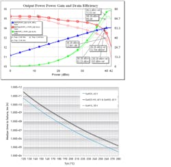
RF engineers, and in particular PA designers, are concerned about device heating and operating temperatures because of the effect on device reliability and performance. The dc power that PAs don’t convert into RF energy is converted into heat, and the electrothermal effects impact RF performance with the dominant drain-lag effect dependent on both the voltage bias and the channel temperature. Device channel temperature is a primary source for thermal degradation mechanisms, leading to shortened device lifetimes (Fig. 1).
GaN transistors provide higher output-power densities, wider bandwidths, and improved dc-to-RF efficiencies than their GaAs counterparts. However, to take advantage of this enhanced performance, designers need to accurately capture the complex behaviors of the device during circuit simulation, including thermal effects generated by the GaN device itself. Among the trapping effects related to channel temperature in aluminum GaN HEMTs are transconductance frequency dispersion, current collapse, gate- and drain-lag transients, and restricted microwave power output.
Furthermore, as with all semiconductor devices, the reliability of silicon-on-carbide (SiC) MESFET and GaN HEMT devices depends directly on maximum operating channel temperature. It’s therefore important to determine with a high degree of confidence what the maximum channel temperature is under specific operating modes—particularly for products operating under continuous-wave (CW) conditions and dissipating large amounts of thermal energy. When designing PAs, it’s crucial that the transistors operate below their rated operating junction or channel temperatures to ensure that the amplifier will have the desired reliability.
How much heat can be generated by a typical high-power GaN PA that might be found in a base station? A GaN HEMT, for example, with gate periphery of 28.8 mm operating at a drain voltage of 28 V delivers 120 W of CW power. At a 60% dc-to-RF conversion efficiency, there will be 80 W of dissipated heat, which translates into a heat density of over 20 kW per square inch.
This heat will be dissipated from the device channel to the package and PCB though structures such as wire bonds, grounding vias, and the semiconductor and package materials themselves. Designers need to ensure that the device is operating below the rated operating junction temperature. Thus, they’re interested in knowing that value and lowering it, if possible, through structures such as wire bonds, grounding vias, and heatsinking strategies, all of which can be optimized through analysis.
Thermal Analysis for RF Applications
Heat maps illustrate device-generated hot spots and the thermal challenges posed by densely packed electronics. Within the IC, performance can be compromised by rises in temperature. In packages/PCBs, thermal problems arise due to Joule heating, which affects IR drop and performance. In the broader system context, we need to identify hot spots and implement a cooling strategy.
To study the temperature resulting from power dissipation, thermal-analysis tools can be combined with nonlinear RF circuit simulation tools to provide the needed power-dissipation information. When combined, the RF circuit simulator and thermal-analysis software provide critical operating temperature information for both in-design and signoff.
A simple thermal resistance network, shown superimposed over a cross section of a die in a package in Figure 2, helps illustrate heat flow in a quad flat no-lead (QFN) package. The PA MMIC is embedded in the QFN package, which is sitting on top of the PCB.
The thermal circuit has a heat source with the power (Q) flowing from the junction to the bottom case of the package, then to the outside world (ambient temperature). Some of the heat will flow from the junction to the case of the package and spread into the board, and then out through the air or some other conduction path.
The thermal version of Ohm’s law shown at the bottom of the diagram is used to calculate the channel temperature of the PA MMIC, which is equal to the power dissipation times the thermal resistance plus the case temperature that could come from the thermal model results. We can obtain a much more rigorous and accurate prediction of temperature through 3D planar modeling of the devices, with material conduction properties and simulated power dissipation coming from nonlinear harmonic-balance (HB) circuit simulation.
Integrated Thermal-Analysis Workflow
RF designers using software that offers multiple integrated tools can obtain operating temperature and heat maps of their RF device, package, and PCB system with direct access to the thermal solver through the circuit simulator. The tools perform their schematic simulations, produce power dissipations, and then automatically generate a thermal model and simulations.
Cadence's Celsius Thermal Solver, for example, offers finite-element analysis (FEA) to accurately determine the operating temperature using an adaptive meshing algorithm. The algorithm works with the Celsius Thermal Solver’s workbench to illustrate thermal heat mapping and automatically report the operating temperature for all defined heat sources in the AWR Design Environment platform.
Thermal analysis can be applied immediately during simulation to improve simulation accuracy, including thermal effects, enabling problems to be discovered early on. In addition, the mechanical computer-aided design (MCAD) and power-dissipation data can be handed off in parallel to a mechanical/thermal engineer for final signoff, if needed.
MMIC PA Example
This example demonstrates how integrating the Cadence Celsius Thermal Solver within Microwave Office circuit design software enables thermal analysis of a high-power X-band MMIC PA in a QFN package on a PCB. The design is initially simulated in the APLAC HB solver, after which the power information from all of the devices within the design is sent to the Celsius Thermal Solver. There, the chip is simulated inside the QFN package on a PCB to see how the power is distributed across the different technologies.
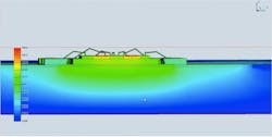
Once the simulation is completed, we can view the full 3D structure (Fig. 3). The power across the board can be seen at upper left and the heat sources spread across the different power transistors of the MMIC at upper right. By turning off the visibility of any of the layers, one may view single layers. The visibility of the package and board structures can be turned off to examine the temperature across the die metallization represented with the heat map (bottom left), as well as with the bond wires made visible (lower right).
The scale for temperature distribution dynamically changes as structures are made visible or removed. The cut setting can be selected to slice the structure for a cross-section view of the localized hotspots in the x, y, and z directions (Fig. 4).
A results summary shows temperatures of the heat sources of the individual field-effect transistor (FET) fingers, which are reported back into the circuit simulator. For this example, the average temperature across each gate finger is 92.6°C for a simulated power dissipation of 2.9 W. This flow enables the designer to simulate closer to the edge of the design space, allowing the PA’s performance to be maximized because a large thermal margin doesn’t need to be left on the table from a safety standpoint. The design also can be studied to see the effects of other options, such as putting the die on a heatsink, on temperature distribution to optimize performance.
Conclusion
This article discussed the importance of thermal analysis for RF power applications. As PCBs become more densely populated with devices, the operating temperatures of those devices impact the reliability (device lifetime) and performance.
A thermal-analysis flow using a thermal solver integrated within the circuit simulator gives designers an understanding of device operating temperatures related to power dissipation. Subsequently, that temperature information can be inserted into an electrothermal model to predict the impact on RF performance. This flow provides RF engineers with ready access to operating temperature data for reliability and performance studies early in the design process.
About the Author
David Vye
Technical Marketing Director, Cadence
David Vye is the senior product marketing manager for AWR software at Cadence, where he’s responsible for product messaging and positioning in the RF/microwave market. A former editor and business development manager for Microwave Journal, David has held a number of technical and marketing positions throughout the RF/microwave industry. He holds a BSEE from the University of Massachusetts at Dartmouth, with a concentration in microwave engineering.
