Algorithms to Antenna: Modeling Mutual Coupling in Large Antenna Arrays
In my most recent blogs, I discussed several approaches to modeling large arrays for 5G communications, with the goal of improving channel capacity (through spatial multiplexing techniques) and realizing cost- and power-efficient systems (through hybrid beamforming). I reviewed multiple methods where the fidelity of the array model was increased by designing an element and generating the resulting pattern with an electromagnetic (EM) solver. We saw this in large phased-array systems by first designing an antenna element and then using pattern superposition to create the pattern for a larger array. We also saw this by designing a smaller subarray, which was then used to build up a larger array.
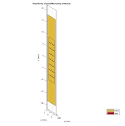
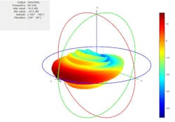
Expanding on this theme, the radiation pattern of an array can be generated from the multiplication of the element pattern and the array factor. However, when an antenna gets deployed into an array, its radiation pattern is influenced by the neighboring antenna elements. This in turn results in mutual coupling. Figure 1 shows one example (from “Understanding Subarray Tradeoffs in Large Antenna Arrays”) of a patch antenna that resonates at 66 GHz. This example was generated using a full solver and includes the effects of mutual coupling between the eight elements.
1. Shown is the structure and pattern for single 8-×-1 ULA.
EM solvers require processing and memory resources that grow very quickly both with the array size and the complexity of the antenna element itself. The desire for higher-fidelity models must be traded off with the time required for simulation. This takes on added significance when the pattern is used in system-level simulations where the overall array pattern needs to reflect beamforming and scanning in the field of view. Fortunately, it is possible to implement techniques that give reasonable simulation times with a sufficient level of fidelity. We will look at two.
Infinite Array Analysis Technique
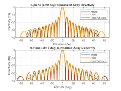
The first technique, referred to as infinite array analysis, can be used to model large finite arrays. Infinite array analysis provides the scan impedance behavior at a particular frequency. This information is used with the knowledge of the isolated element pattern and impedance to calculate the scan element pattern. The large finite array is then modeled under the assumption that every element in the array possesses the same scan element pattern. Figure 2 illustrates a comparison with this type of technique using a full-wave solver based on an array of dipoles.
2. Using a full-wave solver, E- and H-plane comparisons are shown for infinite array analysis.
The pattern plots in the two planes reveal that all three analysis approaches suggest similar behavior; in this example, out to ±40 degrees from boresight. Beyond this range, it appears that using the scan element pattern for all elements in a uniform rectangular array (URA) underestimates the side-lobe level compared with the full-wave analysis of a finite array. This result is likely due to the edge effect from the finite-size array.
Infinite array analysis is one of the tools deployed to analyze and design large finite arrays. The analysis assumes that all elements are identical and that edge effects can be ignored and have uniform excitation amplitude. The example can be customized for different array configurations, but the plots give an idea of how the fidelity levels vary across these types of techniques.
Embedded Element Technique
Another often-used approach to model the mutual coupling effects is embedded antenna element pattern analysis.
The embedded element pattern is the pattern of a single element embedded in the finite array. It is calculated by driving the central element in the array and terminating all other elements into a reference impedance. The pattern of the driven element, referred to as the embedded element, incorporates the effect of coupling with the neighboring elements.
It is common to choose the central region/element of the array for the embedded element, depending on whether the array has an even or odd number of elements (for large arrays, it does not matter). In the code below, this type of pattern can be generated directly based on the center element excitation with the other elements terminated.
The pattern of the isolated element (the radiator located in space by itself) changes when it is placed in an array due to the presence of mutual coupling. This behavior invalidates the use of pattern multiplication, which assumes that all elements have the same pattern. To use pattern multiplication to calculate the total array radiation pattern, and improve the fidelity of the analysis, we replace the isolated element pattern with the embedded element pattern.
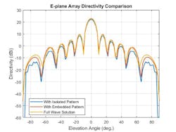
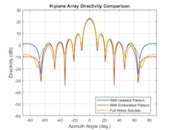
Figures 3 and 4 show example results of the E- and H-field patterns of the isolated element, the embedded element pattern, and the full-wave method-of-moments (MoM)-based solution for the array. The array performance for scanning at broadside as well as off broadside is shown. These results are also based on an array of dipoles.
3. This plot compares different techniques used for E-plane array directivity.
4. H-plane array directivity is compared for a range of techniques.
The pattern comparison shows that the main beam and the first side lobes are aligned for all three cases. Moving away from the main beam shows the increasing effect of coupling on the side-lobe level. As expected, the embedded element pattern approach yields a coupling fidelity level in between those of the full-wave simulation model and the isolated element pattern approach.
Have more questions about the best ways to model the effects of mutual coupling? Email me at [email protected].
Learn more about the topics covered in this blog post:
- Modeling Mutual Coupling in Large Arrays Using Embedded Element Pattern (Example): See how to model mutual coupling with embedded element patterns using Phased Array System Toolbox and Antenna Toolbox.
- Modeling Mutual Coupling in Large Arrays Using Infinite Array Analysis (Example): See how to model mutual coupling with infinite array analysis using Phased Array System Toolbox and Antenna Toolbox.
See additional 5G, radar, and EW resources, including those referenced in previous blog posts.
About the Author
Rick Gentile
Product Manager, Phased Array System Toolbox and Signal Processing Toolbox
Rick Gentile is the product manager for Phased Array System Toolbox and Signal Processing Toolbox at MathWorks. Prior to joining MathWorks, Rick was a radar systems engineer at MITRE and MIT Lincoln Laboratory, where he worked on the development of several large radar systems. Rick also was a DSP applications engineer at Analog Devices, where he led embedded processor and system level architecture definitions for high performance signal processing systems used in a wide range of applications.
He received a BS in electrical and computer engineering from the University of Massachusetts, Amherst, and an MS in electrical and computer engineering from Northeastern University, where his focus areas of study included microwave engineering, communications, and signal processing.
