Series: Ultra-Low-Noise Synthesizer Design
Download this article in PDF format.
Recent years have seen major changes in the frequency synthesis art. Ultra-low-noise discrete VCOs, the heart of low noise synthesizers for decades, now find themselves challenged by integrated VCOs. The best discrete VCOs still enjoy 20-30 dB phase-noise superiority, but IC companies are conducting an asymmetric battle to dominate the market with full integration based not on the best VCO noise, but on architectural innovations that often render free-running VCO noise less important.
This is achieved by putting good VCOs on die, suppressing that noise down to a very low level via feedback, and then dividing down to the application band for a further phase noise reduction. The challenge now facing discrete VCO suppliers is to extend the outstanding phase noise they get in application bands to higher frequency where they also can get the full architectural benefit of the latest synthesizer innovations.
This first article of a five-article series will review modern advanced design methods. This is the online version, which is moderately more complete than the printed version. See the publications page at www.longwingtech.com for considerably more detailed versions of these articles. The next four articles in this series will cover detailed noise analysis (two articles), key parts and tools for low noise implementation, and examples requiring low noise that illustrate current state of the art performance.
Basic PLL Operation and Second-Order Normalized Form
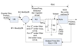
The standard second-order form of PLL design that is presented in most classic text books allows for approximate but still useful design and analysis equations, and a simple description of loop operation (Fig. 1).
1. This is a depiction of the second- and third-order charge pump PLL synthesizer (C1 = 0 for second-order). Frequency is set by firmware via the programmable R and N dividers.
We are used to thinking primarily of voltage and current as the feedback quantities, but in addition to those the PLL also treats phase and frequency as small signal frequency domain variables. When seeking lock over a wide frequency range, the modern phase/frequency detector (PFD) acts as a frequency detector to steer the voltage-controlled oscillator (VCO) towards lock. As frequency converges, the loop transitions to a phase locked mode where phase as a time difference between digital edges is driven to zero.
Since frequency is the time derivative of changing phase (ω = dθ/dt), phase is the integral of frequency. Thus, the VCO acts as an integrator of input voltage to output phase, which introduces −90 degrees of phase shift. That is why its transfer function is in the form Ko / s, the standard frequency domain representation of an integrator. Ko is here given in units of rad/sec/volt. VCO datasheets will normally give Ko in units of MHz/V. To be clear in this article series, we will refer to the Hz/V form as KHz and the radian form as Ko, so Ko = 2πKHz.
With the -90 deg phase shift and the –180 degrees of negative feedback, we only have a maximum of 90 degrees of filtering phase shift allowed before −360 degrees total would result in instability. We normally leave a minimum of 40 degrees of “phase margin” at the loop bandwidth. This margin comes from the zero introduced by resistor R2, as without it the charge pump driving a capacitor would also be an integrator.
Now we may review basic analysis. The classic “phase transfer function” of the loop as given in older references (such as Refs. 8 and 9) is defined here as:
Hclassic(s) is the closed-loop transfer function from the reference input on the phase detector to the feedback input, usually referred to as simply “H(s)” in classic references. This subscript is used to clearly distinguish from the “H” that is used as part of the open-loop transfer function in most modern literature. From the figure above, if we solve for this relationship by “substituting around the loop” using the relations established in the figure, we obtain:
This equation is in a familiar control system form where we may extract standard parameters that aid in understanding and in calculations. The standard normalized form of the second-order system is given by:
The two equations are in the same form, and by equating terms we obtain the following analysis equations:
The term ωn is the “natural” frequency, and is close to but generally not equal to the open-loop bandwidth (see the publications page at www.longwingtech.com for the long form of this article giving the exact relationship between ωn, ζ, and loop bandwidth). When settling, the transient response “rings down” at the natural frequency. The term ζ is the “damping factor” and must be greater than zero for stability. Normally damping factor is set to about 0.5, which will give about 45 degrees of phase margin, or about 0.7 to 1 when an additional filtering pole is added.
Again, referring to Refs. 8 and 9, the common PLL "error transfer function" is defined as:
He(s) may also be represented in the standard normalized form of control theory as:
He(s) is a high pass function, whereas the phase transfer function Hclassic(s) is low pass. It is quickly shown from above that:
It will turn out that many of the modulation and noise responses of PLLs can be conveniently expressed using these functions, which is a great aid in understanding how the loop shapes noise. For example, phase or phase noise variation on the reference input to the phase detector will transfer to the VCO output proportional to the phase transfer function. Since phase transfer function is low pass, above the loop bandwidth there will be suppression of this noise or modulation. The suppression of voltage-controlled oscillator phase noise inside the loop bandwidth will be according to the He(s) function given just above, down to the limits of divider noise, charge pump noise, and crystal reference noise (to be analyzed in articles 2 and 3).
From the analysis equations just above, we obtain the following design equations:
These equations are used to determine R and C based upon chosen values for natural frequency and damping factor. When extra filtering poles are introduced these values will change (particularly the capacitor), but they are still very useful starting points and serve well for many approximations such as settling time, pull out range, and finding minimum possible thermal noise in the loop filter.
The Third-Order Passive Filter PLL
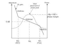
This form is the simplest highly usable form, and is attained by adding another capacitor C1 as shown in Refs 6 and 7. Introducing another filter pole will eventually cancel out the zero. This means that there will be a frequency where phase peaks and then declines (Fig. 2).
2. Shown is open-loop gain and phase in the properly designed third-order PLL. The maximum phase is forced to occur at the loop bandwidth by the design.
The loop filter impedance is:
A half page of circuit analysis will establish:
The open-loop gain function is given by (see figures for G and H):
We know Kd, Ko, and N, and choose loop bandwidth ωL and phase margin ϕm. To find our three unknowns A0, T1 and T2, we need three equations. We get them from the magnitude of GH (which is 1 at ωL), the phase of GH (which gives ϕm at ωL), and the derivative of the phase of GH with respect to ω (which is zero at ωL). This is the basic methodology referred to here as the modern technique.
The magnitude of GH is:
At ω = ωL this magnitude is 1, and we have:
The phase margin expressed as a positive number from 0 to 90 degrees is the difference between the open-loop phase and 180 degrees, which is:
Taking the derivative of phase margin with respect to variable frequency, and setting it to zero at ω = ωL, gives:
We now have two nonlinear equations in the two unknowns T1 and T2. We may solve these numerically, but there is a closed form solution (Ref. 3, pp. 32-36):
Now we may find the circuit values:
The second-order filter (third-order loop) is the lowest noise filter form. However, pushing bandwidth out typically requires additional poles of filtering to keep phase detector noise from contaminating VCO noise.
The Fourth-Order Passive Filter PLL
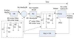
This form uses the third-order filter shown in Figure 3, and is likely the most common filter form.
3. Here are the fourth- and fifth-order PLL forms.
The open-loop transfer function is given by:
The filter (transfer) impedance that is part of the above is given by:
The coefficients A1 and A2 are useful abbreviations for lengthy functions of parts values (see long version).
Using the magnitude function of the open-loop transfer function:
We next define what Banerjee calls “pole ratios,” which shall be selected by the designer based upon factors such as spur rejection. Technically these would be more properly referred to as time constant ratios, but we shall stay with the now established terminology of calling them pole ratios.
T31 is determining how spaced out the added pole is. We must use T31 < 1, and find that 0.5 buys almost all the possible spur suppression that is practically possible.
The phase margin of the open-loop transfer function is given by:
The phase margin occurs at the peak of the phase-margin function. Taking this derivative with variable frequency, and then applying the first derivative test with ω=ωL, gives:
After selecting the pole ratio T31, the above two equations may be solved numerically for T2 and T1, thus allowing T3=T31T1.
Now we come to the “Gamma Optimization Factor” used by Banerjee. This quantity allows approximation, with additional information on its importance given in the long version at www.longwingtech.com. We may extend the earlier expressions for T2 in approximate form to higher-order loops (Ref. 7, 5th ed, p.309), at the same time defining γ:
This parameter is normally close to 1 in practical designs—in the range of 0.7 to 1.3.
Substituting, we get this approximation (leaving the 180 deg. off to convert from phase to phase margin):
The above has only T1 to be solved for. An approximation can be found using tan-1(x) ~ x for small x. The result is:
The other two time constants follow immediately.
When using the approximate approach:
We find A1 and A2 from:
We have the four equations for five values C1, C2, C3, R2, and R3. The method adopted by Banerjee to get a 5th equation is to find the largest C3 that satisfies these equations. The above may be manipulated to find C3:
Applying the first derivative test for the value of C1 that peaks C3:
Everything needed to find C1 is known, and it may be plugged into Equation 40 to find C3. Then the final values are found from:
Passive Filter Fifth-Order PLLs
The addition of an extra RC stage can provide moderate improvement in far out spur rejection over the third-order filter. Speaking very approximately, the benefit of the third-order loop filter over the second is about 2 to 7 dB, while the benefit of the fourth-order filter over the thirdis about 1-3 dB (Ref. 7, 5th ed, p. 324). See the long version of this article at www.longwingtech.com for more details.
Op-Amp Active Filter PLLs
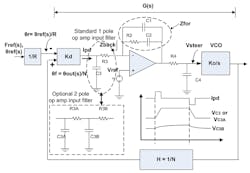
The primary reason for using an op amp is to extend the voltage range of the loop filter to allow VCOs with large tune ranges (since passive loop filters are limited to the relatively low synthesizer IC charge pump output range). This allows for lower Ko and lower noise, as will be shown in articles 2 and 3. The op amp also allows smaller, lower noise resistors and placing the lowest pole after the op amp. There are several topologies for active loop filters, but here a single preferred version (Fig. 4) is given in full fourth-order form.
4. This is the active fourth-order filter and fifth-order PLL, with option for fifth-order filter. This filter is referred to as a “slow slew” active filter, as the input RC reduces speed requirements. Bandwidth limits of the op amp may still make it advantageous to use the two-pole input filter option, converting the filter to fifth order and the loop to sixth order.
A low-noise dc reference voltage is provided at the positive input of the op amp, and the combination of loop action and op amp action will be to keep the negative input of the op amp at this same voltage. In this form the op amp output will “pump up” via current flowing through Zfor to assume whatever voltage is needed to maintain lock. The part values can be selected so that this inverting form suffers only small noise gain (to come in article 2).
For transfer impedance Z(f) we find:
An importance point is that T4 shall be the lowest frequency pole.
We also find:
The open-loop gain as a function of jω is:
Using the magnitude function of the open-loop transfer function (1 at loop BW):
To maintain one set of equations whether f1 or f3 is lower, we refer both higher frequency poles to the lowest pole f4.
To evaluate A0, we need T4 and T2, and then use the selected pole ratios to get T1 and T3. The exact equations are:
The max phase margin occurs at the peak of the phase margin function, where we substitute ω=ωL after taking the derivative in the first derivative test:
Now these two may be solved numerically for T2 and T4, leading then to T1 and T3 via the selected pole ratios (usually around 0.5 for the lowest pole above f4 and 0.25 for the next pole, relative to T4). The below approximations may be used as starting points for the numerical solutions, or used as is.
We may use γ = 1, or alter it from 1 based on the optimization criteria in Banerjee 5th ed, chapter 36. The only variable remaining is T4, which may be solved numerically, or approximately:
If the approximate form is used, then:
In either case:
We now have all the variables needed to find A0 = C1 + C2. We may then find all the part values in Zfor from:
Now we select the values for R3, C3, R4, and C4, which seems easy as we have their time constants, but there are some subtle complexities at work here, including op amp limits to deal with.
On the input side of the op amp it might seem that smaller R3 would help with noise, but actually the opposite is true. The thermal noise of R3 is going up with its square root, whereas its noise gain is going down with R3, so that the noise of R3 on the op amp output is going down with its square root. So, we tend to select the largest R3 that other limits allow, as follows.
Banerjee gives (Ref. 7, 5th ed, p.38) the duty cycle of the phase-frequency detector in frequency-lock mode as a function of the ratio of fref and fout/N as:
In the above flower is the smaller of fref and fout/N. Since most VCOs do not steer far in a fractional sense from their center frequency, the duty cycle would seldom range above 10% (octave-type VCOs being the exception).
Let us define ΔVmC3 as the max filtered voltage change from Vref that we wish to be imposed (such as to comply with op amp input requirements) on C3 during a frequency-lock acquisition event. We may thus write a relationship for R3max as:
Additionally, we need to beware of slew rate limits. Banerjee offers experimental evidence (Ref. 7, 5th ed., pp.371-372) that if the op amp is not fast enough there will be worsening of 1/f phase noise inside the loop bandwidth (typically a few dB). There are four slew rate cases derived in long version (see the publications page at www.longwingtech.com), two in frequency acquisition mode (for lock speed) and two in PLL mode (for noise control). The worst case (highest) requirement on slew rate is usually the frequency-locking case towards the end of the frequency lock process given by:
Furthermore, bandwidth limits of the op amp are an issue, but this can be mitigated by the two-pole input filter option. This allows the op amp to be “cocooned” within filtering that prevents signals beyond its specified bandwidth from reaching it. This would seem to be a more logical strategy than the typical GBW > 10X loop bandwidth that is often assumed with op amp circuits. See the long version for further discussion.
Next, we consider the op amp output current limits on C4. We are used to seeing strict load limits on op amps, but many can drive loads of 10 Ω and even less when those loads are DC isolated, even against large capacitance. But, with a large frequency change on the PLL, that capacitance does take large current that may exceed the op amp max in the range of 10mA to 100mA. Fundamentally, we desire the op amp max current Iopmax to be able to charge C4 at the same rate that Dc*Ipd charges C2 during a large frequency change. Using I*t = CV:
This maximum is sometimes more than we would like to use for reasons of size and cost, and may lead to resistor values too small for the op amp even when dc isolated. In that case we select a value of R4 whose thermal noise is considerably less than the noise of the op amp, and then find C4 = T4/R4.
What’s Next
The transfer function approach shown here is enabling to showing noise sources and shaping in articles 2 and 3, along with showing the key innovations driving full integration, and how discrete VCO makers can fight back. Article 4 will show key parts and CAD tools that are the weapons of the low noise synthesizer designer. Article 5 will put it all together with requirements and examples of integrated and discrete VCO synthesizers to meet them.
Acknowledgments
The author expresses his appreciation for the valuable reviews, comments and information provided by Adnaan Khan, Joe Bouchez of Lonestar III Five Designs, Dean Banerjee at Texas Instruments, C.Y. Teng and Miguel Troester at Taitien, and Ulrich Rohde, Ajay Poddar, and Bill Becker at Synergy Microwave.
Series: Ultra-Low-Noise Synthesizer Design
Farron Dacus is an RF design consultant in Dallas, Texas. He received his BSEE and MSEE from the University of Texas, and he has over 30 years of experience ranging from ICs to circuits to systems in low noise RF, short range radio/IoT, cellular, military communications, and aircraft radios. He may be reached at [email protected].
References
1. “Analyze, Don’t Estimate Phase-Locked Loop Performance of Type 2 Third Order Systems,” Electronic Design, May 1978. This is one of the earliest public references to design with higher-order loop filters.
2. “Digital PLL Synthesis,” National Semiconductor Application Note 335, 1983.
3. Digital PLL Frequency Synthesizers: Theory and Design, Ulrich L. Rohde, Prentice-Hall, 1983. This excellent book is a rare example of a classic reference that presents higher-order loop filters in addition to second-order normalized form, and also presents the closed loop suppression of free running VCO phase noise. Rohde is one of the historical leaders of the frequency source field both in publications and in industry.
4. Microwave and Wireless Synthesizers: Theory and Design, Ulrich L. Rohde, John Wiley and Sons, 1997. This book is an update to the Rohde text just above.
5. “Introduction to Modern Signal Generation; from Analog to Digital: Needs, Advantages, Disadvantages, and “Solutions,” Ulrich L. Rohde, an extensive industry white paper, available from https://badw.de/fileadmin/members/R/3685/6_4_18_UNI_BW_June18-safe.pdf. This reference is particularly valuable for its combination of methods from basic to advanced, and resulting final limits.
6. “An Analysis and Performance Evaluation of a Passive Filter Design Technique for Charge Pump PLL’s,” National Semiconductor Application Note 1001, 1996, by Bill Keese. Though this reference was not the first to analytically present higher-order loop filters, it became widely available via the early internet and had a strong influence.
7. PLL Performance, Simulation, and Design, Dean Banerjee, first edition 1998 and 2001. The focus of this outstanding book is modern design focusing on synthesizers with high-order loops and noise prediction using the normalized noise floor of the particular synthesizer chip to take into account divider and charge pump noise. It is currently in its 5th edition, published 2017, covering sigma delta synthesizers and their spur control methods in high detail. Author Dean Banerjee is an electrical engineer and applied mathematician who was deeply involved in the National Semiconductor effort to build a powerhouse synthesizer IC business (now owned by Texas Instruments), and this groundbreaking book reflects both his detailed insider knowledge and his ability to distill practical design methods with tractable mathematics from the complexity of low noise synthesizer design. The 5th edition of 2017 may be freely downloaded in PDF form at: http://www.ti.com/tool/pll_book.
8. Phaselock Techniques, 2nd Ed, Floyd Gardner, John Wiley and Sons, 1979. A highly respected classic work, though lacking in modern filter and noise analysis methods in early versions. The 3rd edition of 2005 does cover third-order loops (the addition of one filter pole to the second-order form).
9. Phase Locked Loops, Third Edition, Roland Best, McGraw-Hill, 1997. A valuable classic reference, though lacking coverage of higher-order loop filter methods in early editions. The 5th edition of 2003 has a chapter devoted to higher-order loops, and is available online for free download in PDF form at http://ebook-dl.com/book/90836. The 6th edition came out in 2007 and is still in print.
About the Author
Farron Dacus
RF Design Consultant
Farron Dacus is an RF design consultant in Dallas, Texas. He earned a BSEE and MSEE from the University of Texas. Farron has over 30 years of experience ranging from ICs to circuits to systems in low-noise RF, short-range radio/IoT, cellular, military communications, and aircraft radios.
