Download this article in .PDF format
High-frequency GaAs switches are widely used to route signals through RF/microwave circuits and systems. GaAs monolithic-microwave-integrated-circuit (MMIC) switches are the most common type of microwave switch used for communications applications, and they can provide typically fast switching speeds.
However, under certain conditions, longer-than-expected settling times (longer than indicated by the product data sheet) can occur, which can severely degrade system-level performance—especially for packet-based communication systems. These delays, which are relatively unknown to RF/microwave designers, result from a transient effect in GaAs MMIC switches. Fortunately, solutions are not difficult to achieve, once the problem has been properly identified. This holds especially true for systems involving multiple dc and RF/microwave signal sources.
GaAs MMIC switches rely on field-effect transistors (FETs) for their functionality. A FET has three terminals: gate, drain, and source. The main current path or channel is between drain and source, while the gate operates as a control terminal. In a GaAs FET amplifier, input signals are applied to the gate while the output is available at the drain, with the source typically connected to ground.
But in a switch, a FET behaves like a voltage-controlled resistor, with drain and source as conducting terminals and the gate as control. The two conducting terminals are essentially symmetric with respect to the gate, so the distinction between source and drain is not overly important in a GaAs FET switch. The gate controls the two logic levels or switch states of the resistor device: “on” when resistance is low and “off” when resistance is high.
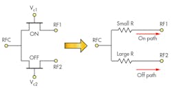
1. The two FETs are combined to form a switch circuit, with its equivalent circuit also shown.
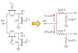
Figure 1 shows a simple circuit of two FETs for realizing a switching function. Some low-cost RF/microwave switches are constructed with this simple configuration, although a series FET in its off state does not yield very high switch isolation. Isolation can be increased by adding a shunt FET in its on state (Fig. 2).
Adding a small shunt resistance to the large series resistance (Fig. 2b) can further increase the signal attenuation of the off signal path, increasing isolation. For the on signal path, the shunt FET is set to its off state, corresponding to a configuration with a small series resistance and a large shunt resistance. The large shunt resistance has negligible effect on the on-path insertion loss.
GaAs MMIC switches have evolved with time. Pseudomorphic high-electron-mobility-transistor (pHEMT) active devices and other technology now offer improved performance compared to earlier GaAs FETs. These devices operate in depletion mode where a negative gate voltage with respect to drain source is required to turn off the channel or, in terms of switching functionality, a negative voltage is required to turn transistors to their off states.
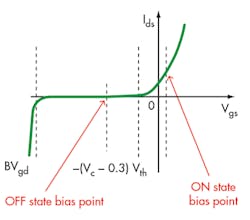
Figure 3 plots a typical transistor drain-source current, Ids, versus gate-source voltage, Vgs, with Vth representing the threshold voltage above which the transistor becomes a conductor. For switch applications, the on state is achieved by biasing Vgs slightly positive, while the off state is achieved by setting Vgs below Vth. Detailed analyses of transistors operating in switch applications are available in the literature.1,2
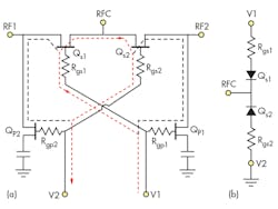
Figure 4 shows how dc bias is established for the on and off transistor states in a GaAs MMIC switch consisting of series and shunt FETs. The gate resistors Rgs1, Rgs2, Rgp1, and Rgp2 are mainly for isolation of RF paths from the dc supply, and they normally have a value of about 10 kΩ. The source capacitors in the shunt FETs (Qp1 and Qp2) are used for blocking dc to ground and providing an RF short.
These capacitors require only moderate values to achieve a low impedance to ground at higher frequencies. This is due to the fact that the equivalent impedance of the series transistors in their off state is usually high enough for good low-frequency isolation. The behavior of the dc currents from the gate to the drain and source of a pHEMT can be modeled as a diode with the gate serving as an anode.
When the diode is forward biased (the gate voltage is positive with respect to the drain/source), the channel is conductive and the transistor is in its on state. If the diode is reversed biased (below the threshold voltage), the channel is open and the transistor is in its off state. Since the circuit is symmetric with respect to control logic levels Vc1 and Vc2, only one logic configuration need be considered, where Vc1 equals the high (H) state and Vc2 represents the low (L) or grounded state.
Figure 4a displays the dc current distribution and flow for the assumed logic configuration. The gates for transistors Qs1 and Qp1 are forward biased, while the gates for Qs2 and Qp2 are reverse biased, corresponding to a switch configuration of on for the RFC-to-RF1 path and off for the RFC-to-RF2 path. There are three main current paths from pin Vc1 (logic high) to pin Vc2 (logic low). Although a full circuit analysis is possible, only one path (Vc1→ Qs1→Qs2→Vc2; the red dashed line) will be considered at this time.
Figure 4b shows the dc equivalent circuit for this current path, where the transistors have been replaced by two diodes that are forward and reverse biased, respectively. This simplified equivalent circuit is for dc bias consideration only; the equivalent capacitances between the drain/source and gate, which in fact are partially short at RF frequencies, are not included. One of the RF ports, RFC, is between the two diodes. The dc voltage at the RFC port is lower than logic high Vc1, roughly by the amount of a forward voltage drop for the diode (which is typically about 0.3 V for the FETs used in MMIC switches).
A similar analysis will show that the dc voltages at RF ports RF1 and RF2 are essentially the same as that at the RFC port. For the other switch logic configuration, where Vc1 is low and Vc2 is high, the voltages at all RF ports are effectively unchanged. For a steady-state condition, the dc voltages at the RF ports are about 0.3 V less than the logic high level, regardless of the logic configuration.
For a FET switch to function properly, each FET must be biased according to design specifications, and any external dc voltage present or resistive load on the internal dc bias current paths will impact the bias conditions for a FET switch’s active devices. For this reason, a dc blocking capacitor must be used at all RF ports to isolate the internal dc bias circuitry from external circuitry surrounding the switch.
The choice of dc blocking capacitor is usually based on the switch manufacturer’s recommendations. But when the settling time for a FET switch’s dc bias is much longer than the switching speed specified in the switch’s data sheet, the choice of dc blocking capacitor should be reconsidered. A long settling time for the dc bias condition can also result in long delays for the RF output power of the switch to reach a steady-state condition, a problem for many modern communication systems.
Figure 5 shows a case where an RF switch can have a potentially long settling time at its output port. It is an antenna diversity application where the output port of a power amplifier (PA) is connected to a single-pole, double-throw (SPDT) switch. The switch’s two output ports are connected to two antennas. The PA is powered by an external supply, VPA, at the RF output pin through an inductor choke. This is a standard bias scheme for RF transistors and is also widely used for various RF PA ICs. In this case, a dc voltage is present on the RF signal line.
Normally, dc blocking capacitor Cblk should be sufficient to protect the switch’s bias circuitry from interference caused by the PA’s supply voltage. However, for improved efficiency, the PA’s power supply is often programmed to turn on before the start of an RF transmission and turned off at the end of the transmission. The PA’s turn-on process will cause a sudden change in voltage on the switch side of the blocking capacitor, with charge movement inside the switch to and from the Vc1 and Vc2 pins.
If the switch control logic is set before VPA starts, the bias condition of the switch will be disturbed by the onset of VPA, which may affect the switch’s performance in terms of settling time. If the switch has not settled before the arrival of an RF signal, system performance will be degraded. The actual settling time will be determined by the time for charge buildup on Cblk according to a new steady-state voltage across the capacitor. Although this transient phenomenon is strongly correlated to the switch’s characteristics, several other factors will affect the settling time, which therefore cannot be fully characterized by switch specification.
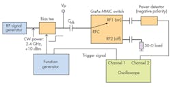
Figure 6 shows a measurement setup for analyzing these transient effects on GaAs FET switch settling time. Although the induced transient voltage on the RF ports is expected to be the root cause of the unsettling condition of RF performance of the switch, it is difficult to directly probe the voltage on the RF ports without introducing loading effects for both the dc voltage and RF signals. From an application perspective, the most relevant concern in this case is RF performance—notably insertion loss—and it is insertion loss, rather than dc voltage, that is monitored with this test setup. A 2.4-GHz signal is applied to the switch’s RFC port with supply voltage to the switch port held steady at Vc = 3 V dc. A power detector monitors RF power at RF1, while RF2 is terminated with a 50-⦠load.
To simulate the PA supply, a step function from the function generator is injected at the outside of the dc blocking capacitor (Vp in Fig. 6). A bias-T isolates the RF path from the function generator. The choke inductor of the bias-T slightly slows the rise time of the step function to about 1 μs, which is still insignificant compared with the settling times observed in the experiments.
Referring to Fig. 4, the RFC port is essentially connected to RF1 port through Qs1 which is in the ON state (RF2 is isolated from RFC because Qs2 is in the OFF state). Therefore, in principle, the capacitance values of Cblk on both RFC and RF1 ports will affect the transient characteristics of the switch in this specific logic configuration. For simplicity, the same capacitance value is used for all dc blocking capacitors in the experiments.
The charging/discharging process in this case is similar to the transient behavior of a resistive-capacitive (RC) circuit with a step-function stimulus. But unlike an RC circuit, the dc bias circuit of a switch is nonlinear. In addition, the step response being considered here is the RF power or insertion loss at the switch output, rather than voltage. While the insertion loss is strongly affected by the switch dc bias condition, the quantitative relationship between the two parameters is not obvious.
As a result, the settling time cannot be easily calculated using an RC time constant. Nevertheless, it is expected that the resulted settling time of the RF output power is strongly influenced by the Cblk value and the equivalent impedance (the ratio of voltage to current) of the transistor bias circuit.
For these experiments, an SPDT GaAs MMIC switch was used, specified to 3 GHz with relatively low output power at 0.1-dB compression rating of P0.1dB = +23 dBm. The device has low supply current of about 5 nA. Such a switch is suitable for battery-powered, short-range wireless applications.
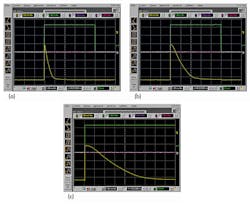
Figure 7 shows the responses of output RF power to a step function for three different Cblk values. The power detector has negative polarity, so any drop shown on the oscilloscope corresponds to an increase in RF power. The amplitude of the step function, Vstep, was chosen to be the same as the switch supply voltage of 3 V.
In response to the step function, the RF power initially drops about 10 dB, indicating a severe disturbance in the dc bias condition inside the switch due to the step function at the RFC port. After this initial drop, the RF power gradually recovers to a steady-state level. The time intervals between the onset of the step function and the point when RF power is fully recovered are used as the time constant in this measurement. They are 1.5, 3.5, and 9 ms for Cblk= 8, 22, and 56 pF, respectively.
The order of magnitude of the measured time constants is in reasonable agreement, with a calculation using RC as time constant if R is taken as the equivalent impedance for a steady-state condition. The measured results confirm that the time constant is roughly proportional to Cblk, at least in the range of capacitance values studied in the experiments.
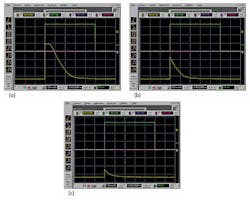
The impact of the amplitude of the step function, Vstep, was also examined with a series of measurements using additional values of Vstep=1.4, 2, and 4 V for Cblk=22 pF. As expected, the magnitude of the initial drop in RF power is strongly affected by Vstep, but the transient time constant remains essentially the same (Fig. 8).
For a true RC circuit, the step responses at the rising and falling edges are expected to be symmetric with respect to the steady-state value, but this is not the case here. The rising edge of the step function causes a considerable drop in RF power at the switch output (Fig. 7a), while the falling edge of the step function has no discernible effect. This asymmetry can be attributed to the characteristics of diodes in the equivalent circuit (Fig. 4b). At the rise of the step function, the increasing voltage on Cblk pushes electrical charges (positive) away from Cblk and into the switch.
The discharge paths are through transistors Qs1 and Qs2, both are in reverse-biased condition with RFC as the reference point. The equivalent impedance in this direction is very high, resulting in a long settling time. On the other hand, at the falling edge of the step function, charge flows in the opposite direction through a forward-biased diode. The equivalent impedance is much less in this direction, and the corresponding transient process is negligible. In this direction, the time constant essentially equals the switching speed quoted in the data sheet for a GaAs MMIC switch.
To analyze the effects of equivalent impedance on an RC circuit, a different switch was used in the experiments—one with higher supply current and much lower equivalent impedance, a model CG2185X2 SPDT switch from CEL. It is a medium-power GaAs MMIC switch suitable for wireless applications to 6 GHz. The supply current used in experiments with this device was 1.9 µA, or about 400 times larger than the supply current used previously.
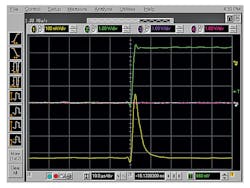
Figure 9 shows the step response for this device using the same conditions for the higher-impedance device in Fig. 7. The initial power drop is similar to the earlier device, but the settling time is much shorter, at about 10 µs.
This confirms that the equivalent impedance indeed affects the transient behavior in a similar manner as resistance in an RC circuit. It also explains why problems with longer settling times are more prominent with low-power switches with lower supply currents (i.e., higher equivalent impedances). Of course, the low-current requirements of such switches makes them well suited for low-power wireless systems where long battery life is important. RF designers concerned with long switch settling times in a system should pay attention to the design of power-sequencing functions in that system.
Power sequencing of RF components such as PAs can also be a concern for the reliability of GaAs MMIC switches. A low-power GaAs MMIC switch may be rated for maximum control voltage of around 6 V and run at actual control voltages as high as 5 V. Since the voltage on the switch’s RF ports is typically below the control voltage by about 0.3 V, the dc voltage on the RF ports can be close to a switch’s maximum rating, especially if a relatively high control voltage is used.
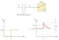
Figure 10 shows a case where the transient voltage on an RF port of a switch, Vs, induced by a voltage step function, Vp, can momentarily exceed the maximum rating of the switch supply voltage. The step response of Vs can be analyzed by realizing that at the onset of the step function, ton, the voltage across the dc blocking capacitor remains unchanged, and subsequent charging/discharging of the capacitor brings the voltage back to the steady- state level.
With ton, the voltage Vs, in response to the step function Vp, jumps by the same amount as Vstep and then returns to its steady-state level through an RC-like discharge process on Cblk (Fig. 10). Even though the voltages on the RF ports are only briefly beyond the maximum rating, the condition can cause long-term performance degradation—if not immediate damage—to the switch. The situation can be avoided by delaying switch biasing until after the step function (such as PA power sequencing).
Mouqun Dong, RF Applications Engineer
California Eastern Laboratories Inc., 4590 Patrick Henry Dr., Santa Clara, CA 95054; (408) 919-2500
References
1. Inder Bahl, Control Components Using Si, GaAs, and GaN Technologies, Artech House, Norwood, MA, 2014.
2. N. Jain and R. Gutmann, “Modeling and Design of GaAs MESFET Control Devices for Broadband Applications,” IEEE Transactions on Microwave Theory & Techniques, Vol. 38, No. 2, February 1990, pp. 109-117.
This file type includes high resolution graphics and schematics when applicable.

