CMOS LNA Serves Flat Gain To 5 GHz
Amplification is an important part of any communications system, and particularly challenging to achieve in broadband and ultrawideband (UWB) communications. To serve those applications, the authors designed a broadband amplifier capable of flat gain from 3 to 5 GHz using a commercial 0.18-μm silicon CMOS semiconductor process. A shunt inductor was used for flat gain and wideband impedance matching, along with a common-gate structure for the input match and a source follower for the output match. Current-reuse helped boost gain while minimizing power dissipation.
The proposed low-noise amplifier (LNA) operates from a +1.8-VDC supply and delivers 21.83-dB power gain with only 0.15-dB variation. The average noise figure is 5.4 dB while the input-referred output power at 1-dB compression is -19 dBm. The LNA achieves input and output reflection coefficients of -13.3 and -19.5 dB, respectively.
The drive for increased data is encouraging the spread of UWB communications systems across the 3.1-to-10.6-GHz range, with a low band from 3.1 to 5.0 GHz and a high band from 6.0 to 10.6 GHz.1 An LNA is a key component in these systems, and must provide flat gain across these wide frequency ranges with good linearity and low noise figure. Silicon CMOS technology provides one avenue for achieving these LNA attributes—in this instance, utilizing the commercial foundry of Taiwan Semiconductor Manufacturing Company Ltd. (TSMC).
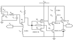
The proposed LNA incorporates a common-gate input matching circuit, common-source amplifier stage with shunt inductor, and current-reuse topology (Fig. 1). The combination of structures and its biasing circuit contribute to its high, flat gain. The circuit was designed and simulated based on TSMC’s 0.18-μm RF CMOS process.
1. This block diagram shows the components used in the UWB LNA circuit.
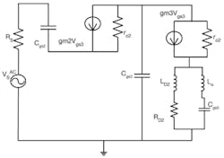
The cascade structure helps provide high gain, even with the lower gain of the common-gate first stage. As shown in Fig. 1, transistor M2 provides high gain, while transistor M3 helps reduce the Miller effect induced by gate-drain capacitor Cgd on M2. This decreases interactions between the output and input ports and contribute to higher gain and better frequency response. Figure 2 provides a small-signal equivalent circuit with loaded parasitic circuit elements for M2.
2. This is a small-signal equivalent-circuit version of the LNA, which incorporates loaded parastics over device M2 for the amplifier stage.
The cascade stage contributes to inductive shunt peaking to enhance LNA bandwidth.2 The shunt peaking inductance and parasitic capacitance CD3 in the drain of transistor M3 work at a harmonic frequency of 4 GHz, according to the relationship:
ω = 1/(LD2CD3)
From Fig. 2, the transfer function of this stage can be presented as follows:
To reduce the parasitic capacitance, the size of device M3can be reduced. The low resistance, RL2, at about 55 Ω, can result in flat gain over the full band from 3 to 5 GHz.
Earlier work3 detailed a relationship between transistors M2 and M3 capable of reducing the noise figure. In this relationship, the width of the cascoding transistor, M3, is chosen to be three times less (this ratio may vary slightly during computer simulations) than that of input transistor M2. In the current report, the width of transistor M2 is 200 μm while the width of M3 is 60 μm.
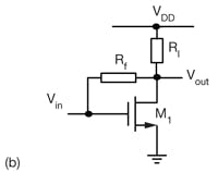
3. These diagrams show (a) the elementary diagram of the LNA and (b) a resistor shunt feedback structure.
An increase in amplifier gain usually comes at a cost of higher dissipated power. But the current-reuse technique can increase gain without an increase in power dissipation. As Fig. 1 indicates, a type of current-reuse approach was adopted for this LNA design. The configuration is based on the resistor shunt-feedback structure shown in Fig. 3(b), with an elementary diagram of the resistor shunt-feedback structure shown in Fig. 3(a). According to that diagram, the input impedance can be expressed as:
Zin = RF/(1 + A)
From Fig. 3(b), transistor M1 and lead resistor RL account for the forward gain, A. In addition, the input impedance (Zin), the voltage gain (AV), the noise factor (F), and the -3-dB bandwidth (BW23dB/sub>) in Fig. 3(b) can be approximated by:
For increased voltage gain and improved noise factor, feedback resistor Rf should be increased, which will decrease the bandwidth. In such a case, the current-reuse configuration is used to achieve improved gain and noise factor. By stacking both NMOS and PMOS transistors—that is, by employing the current-reuse method shown in Fig. 1—the overall equivalent transconductance of the circuit is changed from simply gmN to the combination of the two devices, gmN + gmP. This increases the voltage gain and results in wider bandwidth for the LNA.4
For maximum power transfer and minimal reflections, the input impedance of the first-stage cascade amplifier should be impedance matched with the source impedance, RS = 50Ω. The most common matching circuits for this purpose are inductance-capacitive (LC) network matching and common-gate-stage matching. For good power matching and wideband noise characteristics, broadband input impedance matching can be accomplished by an input common-gate stage or 1/gm termination.
The noise performance of an LNA is dependent on the quality of its input impedance matching, so optimized noise characteristics for the amplifier should be calculated. This involves adopting an optimal relaxation factor, WoptP in the power consumption limit. Parameter WoptP can be approximated by:
where:
COX = εOX/TOX;
RS = 50 Ω;
ω = 4 GHz; and
COX can be calculated based on the parameters of TSMC’s 0.18-{LC MU}m CMOS process.
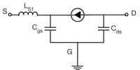
4. This is a small-signal equivalent circuit of the LNA.
An approximation of WoptP with effective results is 165μm. A small-signal equivalent circuit for a common-gate stage with an input inductor, LS1, is shown in Fig. 4. After neglecting the loading effects of the other amplifier stages, the input impedance can be simplified as:
where:
gm1 = the transconductance of M1, and
Cgs1 = the gate-to-source capacitance of M1.
As the frequency increases, the input impedance is close to 1/gm1, which dominates the magnitude of input impedance Zin during operation at gigahertz frequencies. The input inductor (LS1) is used to match with the source impedance of 50 Ω, while the load resistance (RL1) supplies the bias voltage to the second stage of the LNA.
Neglecting induced gate noise, the noise factor of the basic LNA can be given by:
F = 1 + (γ/α)
where γ and α represent empirical process- and bias-dependent parameters, respectively. The noise figure, which is higher when induced gate noise is taken into account, is above 4.8 dB for short-channel devices and will be significantly worse at higher frequencies.5
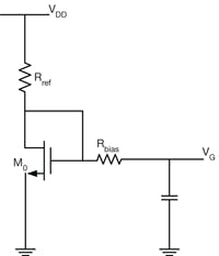
5. This is the bias circuit used with the LNA.
The biasing circuits for the LNA are shown in Fig. 5. The bias voltage can be calculated by the following relationship:
Vbias = Ron/(Ron + Rref)
where:
Ron = 1/gm
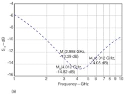
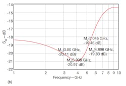
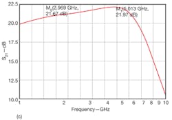
6. The S-parameter performance plots for the LNA show (a) S11 (b) S22, and (c) S21.
The proposed 3-to-5-GHz CMOS LNA was simulated with Spectre RF from Cadence Design Systems based on parameters for TSMC’s 0.18-μm CMOS technology. Figures 6(a) and 6(b) show the S11 and S22 responses for the LNA. The amplifier’s input and output impedance matching are good: less than -13.3 and -19.5 dB, respectively. As shown in Fig. 6(c), the power gain (S21) ranges from 21.67 to 21.97 dB from 3 to 5 GHz.
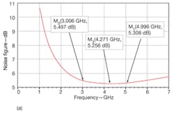
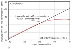
7. These plots show (a) noise figure (NF) and (b) output power at 1-dB compression (P1dB) versus frequency.
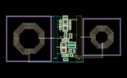
The minimum noise figure in Fig. 7 is about 5.26 dB, while the maximum is about 5.5 dB. Linearity, in terms of input-referred 1-dB compression point (P1dB), is -19.0 dBm as shown in Fig. 7(b). The LNA consumes 47 mW power from a +1.8-VDC supply. Figure 8 shows the layout for the proposed LNA circuit, which occupies an area of only 0.473 mm2.
8. This is a layout of the proposed LNA.
In summary, a CMOS LNA was developed for use in UWB systems. It employs active input and output impedance matching and a shunt inductor for flat gain from 3 to 5 GHz. Implemented in a standard 0.18-μm CMOS process, the LNA achieves an average power gain of 21.8 dB, -19 dBm output power at 1-dB compression, minimum noise figure of 5.26 dB, with input and output impedance matching of -13.3 and -19.5 dB, respectively. While its noise figure is high, the amplifier provides advantages of good input/output impedance matching and broadband gain flatness.
Wang Wei, Professor
Zhao Ying Gong, Graduate Student
College of Electronics Engineering, Chongqing University of Posts and Telecommunications, Chongqing 400065, People’s Republic of China
References
1. United States Federal Communications Commission (FCC), “Final Rule of the Federal Communications Commission,” 47 CFR Part 15, Sec. 503,” Federal Register, Vol. 67, No. 95, May 2002.
2. T.H. Lee, The Design of CMOS Radio-Frequency Integrated Circuits, 2nd ed.,
Cambridge University Press, Cambridge, UK, 2006.
3. M. Reja, et al., “A New CMOS 3.1-11.7-GHz Low Power LNA for Ultra-Wideband Wireless Applications,” IEEE International Symposium, May 27-30, 2007, pp. 1453-1456.
4. T. Taris, et al., “A Low Voltage Current Reuse LNA in a 130-nm CMOS Technology for UWB Applications,” Proceedings of the European Microwave Conference, October 9-12, 2007, pp. 1105-1108.
5. T.H. Lee, The Design of CMOS Radio-Frequency Integrated Circuits, 1st ed., Cambridge University Press, New York, NY, 1998.
6. C. Garuda, et al., “A 3-5-GHz Fully Differential CMOS LNA with Dual-Gain Mode for Wireless UWB Applications,” 48th Midwest Circuits and Systems Symposium, August 7-10, 2005, Vol. 1, pp. 790-793.
7. C-P. Chang, et al., “0.18 {LC MU}m 3–6 GHz CMOS broadband LNA for UWB radio,” Electronics Letters, June 9, 2005, pp. 696-698.
8. S. Vishwakarma, et al., “Ultra Wideband CMOS Low Noise Amplifier with Active Input Matching,” International Workshop on CMOS, May 18-21, 2004, pp. 415-419.
9. T. Taris, et al., “A Low Voltage Current Reuse LNA in a 130-nm CMOS Technology for UWB Applications,” Proceedings of the European Microwave Conference, October 9-12, 2007, pp. 1105-1108.
