This file type includes high resolution graphics and schematics.
Distributed amplifiers are notable for providing very broadband gain. The concept of connecting parallel gain stages with transmission lines harkens back to 1948; Bill Packard, the co-founder of Hewlett-Packard Co., used vacuum tubes for the gain stages.1 The broadband gain possible with such amplifiers still has a place. Even though many modern monolithic-microwave-integrated-circuit (MMIC) amplifiers are optimized for specific bands, many applications require broadband gain through high microwave frequencies.
Since 1989, Johns Hopkins University (JHU) has offered a MMIC design course. As part of the course, a student has the opportunity to design a MMIC, have the design fabricated by a commercial semiconductor foundry (TriQuint Semiconductor), and later have it tested. Professor Craig Moore, who co-taught the class from 1989 to 2003, used a distributed amplifier that he designed around 1988 as a design example for the course.
An updated distributed-amplifier design using TriQuint’s TQPED 0.5-μm GaAs pseudomorphic high-electron-mobility transistors (pHEMTs) was designed and fabricated along with the student designs for the 2006 JHU MMIC design course. The pHEMTs have higher gain and lower noise than the 0.5-μm GaAs metal-epitaxial-semiconductor field effect transistors (MESFETs) used for the 1988 design. The updated 0.5-μm pHEMT design worked well and was documented in the technical literature2
The distributed-amplifier design was revisited in the Fall 2011 JHU MMIC design course using a high-frequency TriQuint TQP13 0.13-μm pHEMT process. Those updated designs are documented in this article. It should be noted that one of the students in the 2011 class, Andrew King, completed an effective distributed-amplifier design with gain that rolled off gradually from 14 dB at 2.5 GHz to 5 dB at 36 GHz. Depending on the operating frequency, available space, and other factors, the “transmission-line” feeds of the distributed amplifier can be either truly distributed (such as the microstrip in King’s design) or lumped-element, transmission-line equivalent circuits.3 The distributed amplifier described here uses the lumped-element approach.
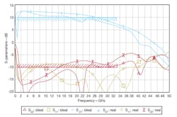
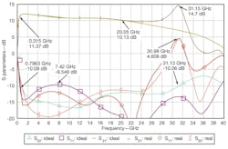
The drain (output) and gate (input) feed lines of the distributed amplifier design are terminated in a 50-Ω resistor. As in the design of ref. 2, a spiral inductor was connected in parallel to the 50-Ω drain termination to reduce DC power consumption. This limits the low-end frequency response to about 1 GHz and, as the design has two decades of bandwidth, the resonance of this inductor causes a slight ripple in the gain (at about 20 GHz) as shown in the preliminary S-parameter simulation (Fig. 1). The simulation compares the amplifier design based on TriQuint’s TQP13 passive elements (real or “lossy” elements), without interconnections, versus ideal lumped-element components (ideal).
1. The S-parameter performance of an ideal distributed amplifier design (thin lines) is compared to a distributed amplifier with real (lossy) TriQuint elements (thick lines).
Originally, an external DC gate bias was to be supplied, but it can be difficult to make a broadband DC supply for a distributed amplifier with two decades of gain. Following a suggestion from Craig Moore, the gate DC supply was simplified by terminating the 50-Ω load resistor to a substrate viahole ground connection to provide a 0-V gate-source voltage (Vgs). This eliminated the flexibility of controlling the drain current, but removed the additional DC bias pad and any resonances that might be created in the gate DC bias supply. For the TQP13 PHEMT process, the 0-V Vgs bias provides good gain, with low noise figure at moderate DC power consumption.
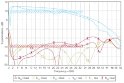
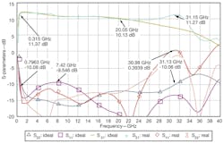
2. The S-parameter performance of a distributed amplifier design with ideal elements (thin lines) is compared to a DC-to-30-GHz amplifier with real elements (thick lines) from the TriQuint process.
This file type includes high resolution graphics and schematics.
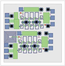
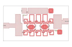
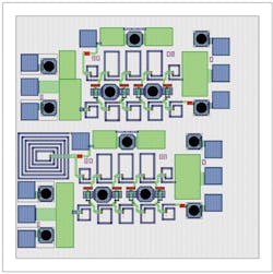
A second, nearly identical distributed-amplifier design was fabricated—one lacking the power-saving spiral inductor on the drain bias. This inductor limits low-end gain to 1 GHz while its resonance causes a midband gain ripple. The resulting DC-to-30-GHz amplifier is less power efficient than the earlier design, since one-third of the 4-V supply is dissipated in the 50-Ω drain termination, but it eliminates the gain ripple of the inductor resonance. Figure 2 offers a comparison of the S-parameters for the original ideal-element amplifier versus the modified DC-to-30-GHz design with real (TriQuint) elements. Figure 3 shows the layouts of both distributed amplifiers on a 54 x 54-mil die. At the top of the die is the DC-to-30-GHz distributed amplifier, with the 1-to-30-GHz version on the bottom.
3. This layout shows distributed amplifier designs for the TriQuint foundry on a 54 x 54 mil die.
Both designs are essentially the same except for the spiral inductor in the drain bias. Electromagnetic (EM) simulation software from Sonnet Software was used to simulate the layout, revealing a potential instability problem at higher frequencies (about 30 GHz)—see Figs. 4 and 5. The chief concern is the relatively large decoupling capacitor on the drain DC bias and its relatively close spacing to the spiral inductors of the drain feed line.
4. This layout plot of the DC-to-30-GHz distributed amplifier was created with EM simulation software from Sonnet Software.
5. This Sonnet Software EM simulation shows the DC-to-30-GHz distributed amplifier with a 31-GHz stability problem.
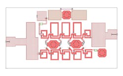
To improve the design, the large 12-pF capacitor was split into two 6-pF capacitors to allow a shorter path to ground for higher-frequency operation, at the same time maintaining the 12-pF total capacitance to benefit lower-frequency operation. Also, the capacitor was moved further from the spiral inductors of the drain feed to reduce parasitic coupling. Finally, ideal 5-Ω resistors on the drain were added in the simulation, significantly reducing the previous instability problem (at around 30 GHz)—see Figs. 6 and 7. Figure 8 shows a modified layout with the modified capacitor and stabilizing resistors on the same 54 x 54-mil die.
6. This is a modified layout plot of the DC-to-30-GHz distributed amplifier, using EM simulation software from Sonnet Software.
7. The simulated performance of the modified DC-to-30-GHz distributed amplifier was generated with simulation software from Sonnet Software.
8. This is a layout plot of the modified distributed amplifier designs based on TriQuint elements on a 54 x 54 mil die.
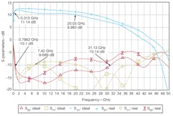
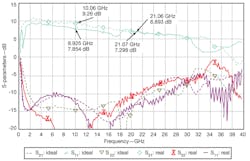
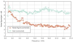
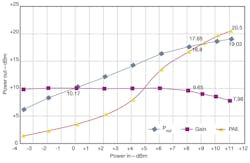
When the student designs were returned from the foundry, it appeared that the original distributed amplifier designs were inadvertently submitted, rather than the modified designs with improved stability. During testing, both distributed amplifiers showed promise at lower bias voltages, as well as at their nominal design voltages, but appeared only conditionally stable at certain intermediate voltages. These oscillations appeared to be well above 45 GHz, but would disappear near the nominal design voltages of 3 V (1 to 30 GHz) and 4 V (DC to 30 GHz) or higher. Figure 9 shows a plot of measured performance for the two designs which differ only by the DC supply bypass inductor. The noise figure and gain were measured at 4-V bias for the DC-to-30-GHz version, showing slightly higher noise figure than expected—but still respectable—at 3 dB from 15 to 26 GHz (the highest frequency measured), as shown in Fig. 10. Figure 11 shows efficiency and output power versus input power for the more-efficient 1-to-30-GHz amplifier at 10 GHz, with 20% power-added efficiency (PAE) at 2-dB gain compression.
9. These S-parameter curves plot the performance of the two different distributed-amplifier designs.
10. These data show the noise figure and gain of the DC-to-30-GHz distributed-amplifier design.
11. These curves show the output power, gain, and PAE of the 1-to-30-GHz distributed-amplifier design at 10 GHz.
Both versions of the distributed amplifier worked well: The 1-to-30-GHz version providing higher output power and efficiency, while the DC-to-30-GHz version had gain below 1 GHz and avoided the gain ripple from the resonance of the DC bypass inductor. There appeared to be some conditional stability concerns, which might make the design less robust over process variations in repeat fabrications. If there is room on a future class fabrication, perhaps the modifications to the layouts that were intended to improve stability can be tested.
John E. Penn, Adjunct Professor
Johns Hopkins University, Engineering for Professionals (EP), 6810 Deerpath Rd., Ste. 100, Elkridge, MD 21075; www.ep.jhu.edu.
RFIC Design, Team Lead
Army Research Labs (ARL), 2800 Powder Mill Rd., Adelphi, MD 20783; www.arl.army.mil.
Applied Physics Laboratory (APL), 11100 Johns Hopkins Rd., Laurel, MD 20723; (240) 228-5000; www.jhu.edu.
Acknowledgements
The author would like to thank TriQuint Semiconductor for their support of the MMIC fabrication for the JHU MMIC design class. Additional thanks are due to Applied Wave Research (AWR), Agilent Technologies, and Sonnet Software for providing design software support for both students and instructors. Also, thanks to the author’s former co-educator, Craig Moore, for his design suggestions. Additional thanks go to Dr. M.L. Edwards for creating the MMIC design course at Johns Hopkins University in 1989.
References
1. E.L. Ginzton, W.R. Hewlett, J.H. Jasberg, and J.D. Noe, “Distributed Amplification, Proceedings of the IRE, Vol. 69, 1948, p. 956.
2. John E. Penn, “Designing MMIC Distributed Amplifiers,” Microwaves & RF, November 2007, http://mwrf.com/semiconductor/designing-mmic-distributed-amplifiers.
3. John E. Penn, “Convert Distributed MICs to MMICs, Microwaves & RF, July 2003, http://mwrf.com/components/convert-distributed-mics-mmics.
This file type includes high resolution graphics and schematics.
