This file type includes high-resolution graphics and schematics when applicable.
Low-noise amplifiers (LNAs) are essential for receiving low-level communications signals, although such amplifiers are typically not broadband in their frequency coverage. However, an innovative LNA design approach blends low- and high-frequency circuit design techniques to achieve low noise from dc to 17 GHz. The amplifier, based on enhancement-mode, pseudomorphic high-electron-mobility-transistor (E-pHEMT) semiconductor technology, achieves low 1/f noise with low harmonic distortion and relatively flat gain across its wide frequency range.
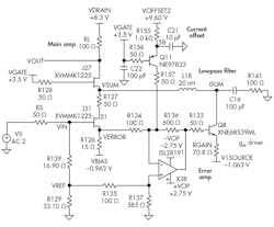
The novel amplifier design (Fig. 1) features a cascode configuration with an op-amp-based error amplifier, transconductance (gm) current driver, lowpass filter (LPF), and active current source to supply a dc offset current to the error amplifier. The amplifier design also includes a 50-⦠resistive divider that serves as an input for the differential amplifier. The LPF isolates the transconductance driver from the cascode at high frequencies and provides a 100-⦠high-frequency termination.
The LNA circuit cascode is formed by E-pHEMTs J27 and J31. Amplifier gain is set by resistor R126 in the source of transistor J31 and load resistor RL in the drain of device J27. For modeling purposes, source resistor RS is used to connect to the gate of transistor J31. The signal at the source of J31 consists of an attenuated version of VIN plus random noise and harmonic distortion.
Resistors R129 and R139 form a broadband 50-⦠voltage divider, with the output of R129/(R129 + R139) = 1/gm + R126, where gm is the transconductance of J31. The output of the voltage divider is connected to resistor R135, one of the input resistors at the positive input port of the error amplifier. This amplifier, X38, is a high-speed op amp with ultralow 1/f noise. It has gain of 6, which is set by the ratio of resistor R136 to R134 and the ratio of resistor R137 to R135.
Transconductance
Bipolar transistor Q8 forms a low-noise transconductance amplifier that drives the source of the common gate of transistor J27 in the cascode. The voltage of the differential error amplifier is applied to the transconductance amplifier to develop an error current that is summed at the source of transistor J27. Passive components L18, C16, and R141 provide isolation for the transconductance amplifier from the cascode, as well as produce a 100-⦠termination at high frequencies for the error amplifier. The transconductance of the error amplifier is set to a first-order value of 14.12 mmho, or 1/70.8 â¦. This is referred to as RGAIN. Inductor L18 has a very high resonant frequency, in the gigahertz range, and provides isolation between the cascode and error amplifier.
In the LNA, Q11 is a bipolar transistor current source that provides an offset dc current to the summing node of the error amplifier, with the offset current set by resistor R155 and a dc supply of +9.5 V dc, VOFFSET2. Capacitor C21 provides a high-frequency ac ground to the emitter of Q11, and resistor R156 provides a high-frequency 50-⦠termination to the base of Q11.
Node VREF contains an attenuated signal, VIN, at the gate of J31, which serves as the reference signal for the error amplifier. The second input signal to the error amplifier is from the emitter of J31, which contains an attenuated version of VIN plus an error signal. The error term consists of harmonic distortion plus random noise.
The output of the error amplifier is the error term multiplied by the amplifier’s gain of 6. This output is then passed through a transconductance amplifier with gain of 14.2 mmho, which converts the signal to an error signal current that is summed into the source of transistor J27.
Testing the Prototype
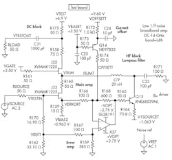
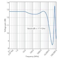
A test board fixture was assembled (Fig. 2) to evaluate the prototype LNA circuit. The load resistor for the cascode was split into two resistors, providing a pickoff of the signal output of the cascode. A number of different measurements were performed to characterize the amplifier for its wideband performance. For example, Fig. 3 shows voltage gain as a function of frequency, with the marker indicating a usable bandwidth of 17.9 GHz.
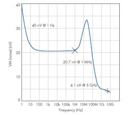
Figure 4 plots the output noise of the LNA from 1 Hz to 10 GHz. The peak 1/f noise of 40 nV RMS occurs at the lowest frequency, 1 Hz. The output noise drops to 22 nV RMS at 10 Hz with the noise remaining flat to 1 MHz. A second peak in the output noise level, at about 33 nV RMS, occurs at 30 MHz. Output noise drops to 4.1 nV RMS at 5 GHz.
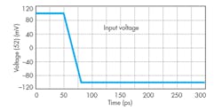
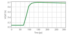
Figure 5 illustrates a plot of the input voltage step at node 52, with impressive 90%-to-10% fall time of 22 ps. Figure 6 is a plot of the output voltage at node VOUT. The step appears to be a dominant pole response, with an output step of less than 30 ps. The output has no ringing and no aberrations appearing 50 ps after the step.
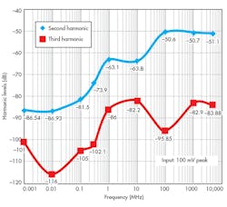
Figure 7 shows second- and third-harmonic distortion as a function of frequency for a peak input of 100 mV. Second-harmonic distortion is –86.54 dBc at 1 kHz, remaining flat to about 10 kHz. The first peak in the second-harmonic distortion curve occurs at –63.1 dBc, remaining flat to about 10 MHz. The second peak in the second-harmonic distortion curve occurs at about –50.6 dBc at 100 MHz, with second-harmonic distortion remaining at about that level to about 8 GHz. Third-harmonic distortion is below –82.2 dBc from 1 kHz to 8 GHz.
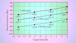
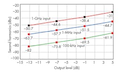
Figure 8 plots second-harmonic distortion in dB as a function of LNA output-power level, for input signals of 100 kHz, 1 MHz, and 1 GHz. For an output level of –13 dB, for example, the second-harmonic distortion is about –82.0 dB at 100 kHz, –63.7 dB at 1 MHz, and –50.7 dB at 1 GHz. For an output level of +5 dB, the second-harmonic distortion increases to –61.9 dB at 100 kHz, –44.7 dB at 1 MHz, and –31.0 dB at 1 GHz.
The novel amplifier delivers impressive noise performance over an extremely wide bandwidth, making it suitable for receivers and other applications from audio through microwave frequencies. The integral error amplifier helps minimize noise, and E-pHEMT active devices enable consistent gain to beyond 17 GHz. The patented design is usable down to dc with stable and consistent gain and noise performance.
