PLL Synthesizer Provides Fast Locking
This file type includes high resolution graphics and schematics when applicable.
Frequency synthesizer lock time is a key parameter in many systems, especially for those in which frequency tuning speed is essential. Short lock times translate into fast tuning speeds and help make signals difficult to track—an important attribute in many military and business operations.
In pursuit of fast locking time, a simplified phase-lock-loop (PLL) frequency synthesizer was developed. It provides low phase noise and low spurious levels based on a dynamic loop-bandwidth technique which has a controllable charge-pump current and dual-charge-pump structure. Its lock time is just 4.8 μs. The phase noise ranges from -100 to -105 dBc/Hz within the loop bandwidth, with spurious suppression of better than -63 dBc for the frequency band of 1.4 to 1.6 GHz.
There are several ways to boost the locking speed of a PLL frequency synthesizer. The preset voltage technique can provide a preset tuning voltage for the synthesizer’s voltage-controlled oscillator (VCO) to tune the oscillator’s output frequency closer to the target frequency and reduce the total time needed for tuning to that target frequency. Because the speed of lookup functions and digital-to-analog-converter (DAC) circuits are in the range of nanoseconds—much faster than the typical locking time of PLLs, which is in the range of microsecond—the preset voltage technique is, in theory, the fastest method available.
However, the control module used with the PLL preset voltage technique is very complex, which can mean increased cost, larger circuit size, and lower reliability. The dynamic loop bandwidth technique changes the loop bandwidth in different stages. It can boost the locking speed while achieving low phase noise and low spurious levels. Yet, switching the loop bandwidth can introduce frequency jitter, which may increase the locking time; the loop bandwidth is limited by the phase comparison frequency of this approach.
The fractional-N technique uses a higher phase comparison frequency which means a wide loop bandwidth and lower division ratio than for an integer-N frequency synthesizer. This approach enables low-frequency phase noise to be suppressed to a high degree.2,3 For optimum performance and fast locking times, the fractional-N and dynamic loop bandwidth techniques were combined. The sigma-delta technique can be applied to help suppress fractional spurious levels, meaning a wider loop bandwidth can be used under steady-state conditions to speed the locking time even more.4,5
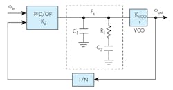
To better understand the dynamic loop bandwidth method for speeding the tuning time of PLL frequency synthesizers, it is necessary to review the relationship between synthesizer loop bandwidth and PLL locking time. A nonlinear relationship describing the loop module is needed to calculate the locking time accurately. Based on a simplified PLL system (Fig. 1), the transmission function of the loop’s lowpass filter can be found from Eq. 1:
where
A0 = C1 + C2;
A1 = C1C2R1; and
T = R1C2.
Because the high-order term has little impact, the system transmission function can be simplified to the relationship of Eq. 2:
with
The locking time for closing the loop6 can be found from Eq. 3:
The loop bandwidth of the second-order filter is ωBW = 2ζωn, so that Eq. 4 can be applied:
When the frequency jumps from 1.4 to 1.6 GHz, the locking time of the structure shown in Fig. 1 with a 600-kHz loop bandwidth and frequency deviation of 10 ppb (10 Hz) can be calculated by means of Eq. 5:
When the loop bandwidth changes to 150 kHz, the locking time can be found by means of Eq. 6:
As the loop bandwidth becomes wider, shorter lock times can be obtained. Because the loop bandwidth is proportional to ωn, and ωn is proportional to (IP)0.5, it is possible to achieve a dynamic loop bandwidth by changing the charge pump current, Ip. The model ADF4154 phase-frequency detector (PFD) from Analog Devices was chosen for the PLL since it has a controllable charge pump current. Its charge pump current can be controlled in 12 grades with a minimum value of 313 μA and maximum value of 5 mA.
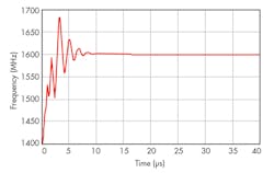
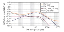
A value of 313 μA was selected as the standard to design the loop structure and control Ip to be 5 mA in fast-locking mode, thus quadrupling the loop bandwidth and achieving fast-locking operation. The design was simulated using the Advanced Design System (ADS) simulation software from Agilent Technologies [now Keysight Technologies], which indicates that the locking time is close to 14 μs (Fig. 2) and the phase noise is -102 dBc/Hz offset 1 kHz from the carrier (Fig. 3).
This file type includes high resolution graphics and schematics when applicable.
The Difference-Loop Advantage
This file type includes high resolution graphics and schematics when applicable.
To further improve fast-locking PLL performance, a difference loop structure was designed with a dual-charge-pump output to increase the locking progress (Fig. 4). The PFD was changed from a model ADF4154 to a model ADF4193, also from Analog Devices. Model ADF4193 is a fractional-N PFD with differential dual-output configuration. The charge pump features 64 parallel charge-pump units, each of which can provide 100-μA current. In fast-locking model, the loop bandwidth of the PLL system increases eight-fold with the full workings of the entire 64 charge-pump units, largely shortening the PLL lock time.
In the system shown in Fig. 4, when the phase error of the two input signals of a PFD increases positively, the charge pump provides the loop filter with a source current which is integrated by the loop filter structure to control the VCO. This source current makes the phase of VCO’s output carrier signal approach the reference frequency phase. Conversely, when the phase error of the two input signals of the PFD increases negatively, the charge pump absorbs the sink current from the loop filter to make the phase of VCO’s output signal close to the phase of the reference frequency via a negative adjustment. The final goal is for the phase error of the VCO’s output and the reference frequency to become zero.
The difference charge pump largely improves the degree of mismatch between the source current and the sink current that will optimize the spurious performance. In doing so, it provides more freedom of design for the loop filter. Moreover, in the design shown in Fig. 4, when the loop bandwidth increases, switch SW3 is triggered to reduce the charging resistance of the capacitance linked to the OPA’s output port. This will lead to an increase in charge current. This reduces the time of reaching a certain tuning voltage even more.
However, the other parameters of the system changed with the loop width—especially the damping factor, which increases with the charge pump current and may also affect the time constant. To keep the damping factor unchanged, it is necessary to adjust R1 proportionally with the change of Ip to stabilize the loop as shown in Figure 4. In this program, switches SW1 and SW2 are triggered to shorten RA2 and RB2 when the charge pump current Ip increases multiply to keep the damping factor unchanged.
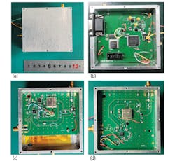
To demonstrate the effectiveness of combining these methods for enhanced PLL synthesizer tuning speed, two PLL frequency synthesizers were fabricated with commercial PFDs. One used a model ADF4154 as the PFD; the other used a model ADF4193 as the PFD (Fig. 5). The lock times of the two synthesizers were compared.
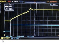
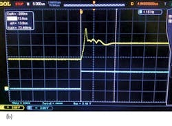
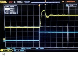
An indirect measurement approach was used to determine the synthesizer lock times. It considers the enable signal LE as the trigger pulse and then measures the tuning voltage with an oscilloscope.7Figure 6 compares the lock times for the synthesizers with (a) a 150-kHz static loop bandwidth and when using (b) the model ADF4154 as the PFD and (c) the model ADF4193 as the PFD. For the static loop bandwidth of 150 kHz and a 200-MHz frequency step, the lock time is 30 μs. This is close to the value of 34.7 μs computed by Eq. 6. This illustrates that Eq. 3 has reference values.
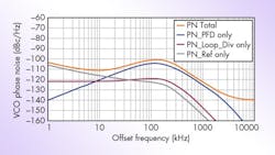
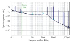
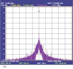
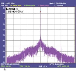
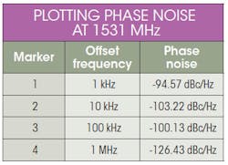
Figure 7 shows the spurious performance for an output frequency of 1531 MHz with a model ADF4193 as the PFD. When the frequency span is 1 MHz, spurious suppression is better than -63 dBc with phase noise performance of -94.6 dBc/Hz offset 1 kHz from the carrier (Fig. 8 and table). Within the loop bandwidth, the phase noise ranges from -100 to -105 dBc/Hz. The maximum spurious level of about -66 dBc occurs at a 1-MHz offset frequency. Fractional spurious signals occur at offsets of 2 and 3 MHz, where the spurious suppress is better than -70 dBc.
In short, Eq. 3 expresses the relationship between loop bandwidth and PLL synthesizer locking time. The dynamic-loop-bandwidth technique was applied to speed locking time; it allows a higher loop bandwidth during frequency tracking to achieve fast locking times. A frequency synthesizer was fabricated with the model ADF4154 PFD that achieved locking time of only 13.8 μs. To further shorten the locking time, a design structure was developed employing the difference between dual-charge-pump outputs to accelerate the speed of changing voltages. By fabricating a PLL frequency synthesizer with the model ADF4193 PFD, a lock time of just 4.8 μs was achieved, and improvement of 9 μs over the design using only the dynamic-loop-bandwidth approach.
This work was supported by the National Natural Science Foundation of China, under grant No. 61001012.
Tang Qing-Hua, Professor
Cui Jun, Master’s Degree Candidate
Zhu Pu-Qing, Engineer
Zhan la-Min, Professor (and corresponding author)
Institute of Microwave Technology Application, Huazhong University of Science and Technology, Wuhan, 430074, People’s Republic of China
This file type includes high resolution graphics and schematics when applicable.
References
This file type includes high resolution graphics and schematics when applicable.
1. W.F. Egan, Frequency Synthesis by Phase Lock (Wiley, New York, 2000), Chapter 1.
2. K. Woo, Y. Liu, and E. Nam, “Fast-lock hybrid PLL combining fractional-N and integer-N modes of differing bandwidths,” IEEE Journal of Solid-State Circuits, Vo. 43, No. 2, 2008, pp. 379-389.
3. M. Moghavvemi and A. Attaran, “Recent Advances in Delay Cell VCOs,” IEEE Microwave Magazine, Vol.12, 2011, pp. 110-118.
4. T.H. Lin, C.L. Ti, and Y.H. Liu, “Dynamic Current-Matching Charge Pump and Gated-Offset Linearization Technique for Delta-Sigma Fractional. Circuits and Systems,” IEEE Transactions, Vol. 56, No. 5, 2009, pp. 877-885.
5. J. Carlini, “Practical Developments Using Today’s Fractional Synthesizers,” 2009, pp. 34-47.
6. Minhua Chen, Jiangxia Li, Xiang Shi, Minghui Yang, and Xiaowei Sun, “Phase-Locked Loop Frequency Synthesizer Based on Lock-Time Analysis,” Journal of Microwaves, Vol. 28, No. 1, 2012.
7. Application Note, “The Measurement of Hopping Time for Frequency Synthesizer,” Aerospace Shanghai, Vol. 4, 2005, pp. 56-59.
This file type includes high resolution graphics and schematics when applicable.
