Analysis of a 24- to 30-GHz Phased Array for 5G Applications (Part 2)
Download this article in PDF format.
Here, we’ll begin by exploring full-wave simulation of the 5-×-16 array shown in Figure 1 of Part 1. The last resort is a numerical simulation of the entire array using commercial 3D full-wave software, such as CST Microwave Studio (MWS), ANSYS HFSS, COMSOL Multiphysics, EMPIRE XPU, etc. All data can also be obtained via testing inside the antenna range. Thus, we can generate an embedded database of 3D patterns and scattering (S) or impedance (Z/Y) matrices for each element in the array.
This approach leads to an outcome with a massive database (see footnote 1 from Part 1) and assumes access to high-performance computers. It’s desirable to implement parallel processing, as well as GPU and cache accelerating.6 All of the numerical simulation data that follows was obtained using CST MWS.
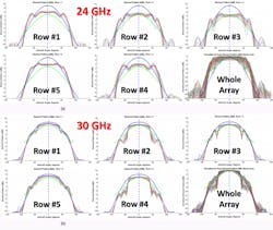
We can start from the active directivity (in dBi) patterns of the elements that belong to the 5-×-16 panel in Figure 1 of Part 1. Remember that the term “active impedance” means that a single array element is driven while all others are connected to dummy loads. The set of plots in Figures 1a and 1b illustrate the patterns of all 80 elements split into the row groups at 24 and 30 GHz, respectively. The red dotted line depicts the averaged pattern for each row.
1. Shown are the active patterns of the 5-×-16 array in rectangular lattice at 24 GHz (a) and 30 GHz (b).
For comparison purposes, the azimuthal cut of the pattern shown in Figure 6 of Part 1 is marked by a blue asterisk symbol. The green circular lines reflect the azimuthal cut of the pattern in Figure 9 of Part 1. Note that the latter is not an active pattern, since the element and an infinite number of its neighbors are uniformly driven.
Pattern Envelopes
As expected, in the ±45-degree angular sector, the element patterns in the rim and next-to-rim rows are practically identical. The set of curves titled “Whole Array” (bottom right corner) shows all 80 patterns being normalized to their peak to demonstrate the shape of the patterns and evaluate the array beamsteering performance. The steepest pattern envelope at 24 GHz describes the no-mutual-coupling element, while the infinite-array element is closed in its shape to the active pattern. In this case, we can expect the overestimated scan loss to be close to the theoretical level of 10 × log10 (cosθscan).6
At 30 GHz, the infinite-array simulation can be considered overoptimistic. A closer look at the active patterns reveals that the patterns are not only different, but mainly asymmetrical relative to θ = 0. The expected consequence is the slim asymmetry in scan loss as the main beam is steered to +θscan or −θscan.
Furthermore, the beams slightly squint to the right or left with the ripples, droops, and overshoots on the top. All such terminology is typical for the analysis of a square-wave passing low-band filter. This similarity is not occasional because both the pattern and signal envelope are formally defined by similar-in-structure Fourier and so-called Fourier-Floquet series.
The pattern envelopes can be described by the set of spatial harmonics, while the signal processing is based on a similar series in the frequency domain. This means that a finite periodic array is somehow equivalent to a low-band filter that “cuts off” the radiation of high-order spatial harmonics and keeps them nearby in the form of reactive fields. Such an analogy not only lets us control the numerical simulation process, but often predicts its outcome without any simulation.
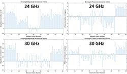
The stem plots in Figure 2 reflect the deviation of boresight active directivity (two left plots) from the peak-versus-element position in the array. Such differences can reach −2.5 dB at 24 GHz and diminish to −0.8 dB at 30 GHz. Finally, notice that the pattern variations are more noticeable at 24 GHz near the lowest resonance because of strong proximity coupling. The plots on the right reveal that the phase of boresight radiation slightly varies within a few degrees. Therefore, to avoid antenna performance degradation, an internal diagnostic and calibration system should be implemented.
2. The deviation of boresight active directivity and phase versus element index number are presented in these plots.
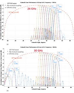
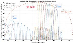
The graphs in Figures 3a and 3b demonstrate the normalized-to-boresight beamsteering up to 45 degrees in azimuth at 24 GHz and 30 GHz, respectively. As predicted, there’s no grating lobe at 24 GHz. The full-wave simulation produces a scan loss of −2.02 dB, while the no-mutual-coupling and infinite-array approaches result in −4.5 dB and −1.5 dB, respectively.
3. Normalized-to-boresight beamsteering performance is revealed at 24 GHz (a) and 30 GHz (b).
At 30 GHz, the full-wave simulation produces a scan loss of −4.0 dB. The no-mutual-coupling and infinite-array approaches result in −2.83 dB and −1.5 dB, respectively. These last two results are overly optimistic.
The same situation exists with respect to predicting the grating lobe level. The full-wave, no-mutual-coupling, and infinite-array approaches predict −2.71 dB, −1.83 dB, and −8.67 dB, respectively, relative to the peak at θscan = 45 degrees. The infinite-array number is certainly too good to believe. Therefore, the accuracy of the scan loss and grating-lobe level should be verified via full-wave simulation.
Boresight Return Loss and Input Impedance
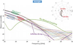
Figure 4 depicts the return loss in dB of all 80 elements driven uniformly in magnitude and phase to form the boresight beam. As predicted from the array symmetry, three sets of curves have comparable frequency dependency: rows 1 and 5 (light blue oval) that mostly include the rim elements, rows 2 and 4 (light green oval) that mostly include the next-to-rim elements, and row 3 (light red oval) that includes the center elements.
4. This graph shows return loss and impedance of elements driven uniformly.
The solid green line is shown for comparison and reveals that disregarding mutual coupling leads to incorrect results. A much better method is the infinite-array approach. As expected, this curve closely follows only the center elements, while purely reflecting the frequency behavior of the rim and near-rim elements. The enclosed Smith chart reveals the input impedance (normalized to 50 Ω). This means that the consistent model platform’s database should include the digital images of a minimum of three essential elements: one from the rim, one from the next-to-rim, and the last from the center elements.
Full-Wave Simulation of 5-×-16 Array with Triangular Lattice (Fig. 2 of Part 1)
Readers can find more detailed data regarding the 5-×-16 array-with-triangular-lattice geometry by visiting the website https://emfieldbook.com. Just several substantial results are presented. The active-pattern deviations become more noticeable not only from element to element, but from row to row. The same is true for the active return loss. Despite this, the input impedances of the elements of the boresight radiating array continue to be well-collimated around the center of Smith chart.
The grating lobe in Figure 5 drops to −6.3 dB as the beam is steered to 45 degrees at 30 GHz. Though not a very significant reduction, it is enough for the scan loss to diminish to −2.83 dB. This is primarily explained by the fact that the element-active patterns become slightly wider in a triangular lattice versus the rectangular lattice. One can notice the increase in side-lobe level relative to the rectangular lattice. For more details and comments, visit https://emfieldbook.com.
5. According to this normalized-to-boresight beamsteering performance result, the grating lobe drops to −6.3 dB as the beam is steered to 45 degrees at 30 GHz.
Conclusions
Now, we possess all of the essential information needed to compare the results using different approaches: no-mutual-coupling, infinite-array environment, and full-wave CST simulation of the array in a triangular and rectangular lattice. All data concerning directivity, scan loss, and grating-lobe level (column 4, after the slash symbol) are summarized in the table.
Referring to the data from Figure 2, we can come to these conclusions:
- Any model can be used to obtain a practically correct estimation of boresight directivity.
- A minimum of three different elements (rim, near-rim, and center) must be considered to reach an accurate scan-performance estimation, especially for the wideband array at a higher end of the frequency band.
- The scan and grating-lobe performance of an array in triangular lattice generally requires the full-wave examination.
- As a rule of thumb, the scan loss/input impedance versus frequency requires the full-wave analysis. Some rough estimation might be obtained using the infinite-array environment model, but that issue needs additional investigation.
Acknowledgment
This work has been encouraged by Victoria Pereira, president of Otava Inc., and partially funded by her company.
Vladimir Volman, Ph.D., is a Fellow and PMS of Lockheed Martin (retired) and a consultant.
References
1. David Vye and Jack Browne, “Platform Propels RF Designs from Concepts to Products,” Microwaves & RF, October 2018, pp. 62-63.
2. Jack Browne, “Bringing mmWave Signals to the Masses,” Microwaves & RF, June 2019, pp. 51-54, 68.
3. Sarah Yost, “First to 5G: Who Will Win?” Microwaves & RF, June 2019, pp. 35-36.
4. Kenneth Puglia, “A Brief Tutorial on Microstrip Antennas (Part 1),” Microwaves & RF, November 2018, pp. 40-62.
5. J.A. Anasari and R. B. Ram, “Broadband Stacked U-slot Microstrip Patch Antenna,” Progress In Electromagnetics Research Letters, Vol. 4, pp. 17-24, 2008.
6. Vladimir Volman and Andrzej Jeziorski, Engineering Electrodynamics. House of Maxwell’s Electrodynamics, 2017, see also https://emfieldbook.com.
7. Constantine A. Balanis, Antenna Theory, 3rd Edition, Wiley & Son, 2005.
8. David M. Pozar, “A Relation between the Active Input Impedance and the Active Element Pattern of a Phased Array,” IEEE Transactions on Antennas and Propagation, vol. 51, No. 9, September 2003, pp. 2486-2489, or see: https://pdfs.semanticscholar.org/4f10/5bda3300308e7771276cf65b6557419f2e1d.pdf
9. John S. Williams, ”Electronic Array Design,” Tutorial, https://intranet.birmingham.ac.uk/eps/documents/public/emuw2/SCF01.pdf
