X-band Push-Push Oscillator Simulation and Measurement (Part 1)
Download this article in PDF format.
Push-push oscillator configuration via harmonic-balance computer simulation and test measurement is the focus of this article series (see footnote at end of article). Specifically, it lays out basic oscillator theory of generated negative resistance and analyzes the common-collector, single-stage oscillator, which is subsequently utilized as a basic building block of the push-push oscillator configuration (that will be covered in the upcoming part 2).
Uncommon aspects of resonator loading and oscillation conditions are explored in this series. Conventional oscillator theory is reinforced via large-signal loading analysis simulation using the single-stage, common-collector oscillator. The unique operation of the push-push oscillator configuration is examined using harmonic-balance simulation of spectral content and time-domain voltage waveforms. Dynamic load lines are investigated and utilized to explore peak signal excursion and degree of nonlinearity. In addition, predictions of power output, phase noise, voltage control, and harmonic content are compared with measured data.
Introduction
The push-push oscillator configuration has been used to extend the frequency of operation of bipolar transistors well into the microwave and millimeter-wave (mmWave) regions. It has sustained service and attractiveness thanks to performance that’s not achievable by other signal-generation methods. Recently, it’s been implemented within SiGe and InGaP HBT technologies.
Several authors have attempted to explain the frequency-multiplication and noise-cancellation properties with limited success.1, 2, 3 A common-collector oscillator is demonstrated to be a fundamental element of the push-push oscillator architecture when implemented with bipolar transistors. The investigation begins with exploration of negative resistance generation, resonator coupling, and loading of the basic oscillator element.
The coupling of oscillator output power is found to profoundly impact power output, load-line, harmonic content, and noise. The push-push oscillator is formed from the back-to-back combination of two common-collector oscillators operating in phase opposition conditions, thereby creating a null at the harmonic output node. Specific aspects of large-signal simulation, device models, and simulation algorithm are discussed with respect to parameter prediction accuracy. Measurement data is presented that correlates satisfactorily with parameters like power output, harmonic content, and phase noise, but less so with respect to operational frequency prediction.
Basic Oscillator Concepts
Several types of oscillators exist: blocking, relaxation, monostable, and bistable are typical of lower-frequency operation. Higher-frequency oscillators are generally segmented within two classes: negative resistance oscillators and feedback oscillators. Gunn and Impatt diode oscillators represent examples of negative resistance oscillators, while feedback oscillators can be characterized as reflection or reaction types. Feedback oscillators create a negative resistance, i.e., Γ > 1.0, due to circuit topology. This presentation will focus on feedback-type oscillators.
The modified Colpitts oscillator is fundamental to sinusoidal signal generation in RF, microwave, and mmWave frequency bands. Figure 1 depicts various configurations of the modified Colpitts oscillator in which alternate terminals of the transistor are grounded and the feedback and resonator networks are represented.
1. Modified Colpitts oscillator configurations include these three electrically equivalent circuit topologies.
In each case, the feedback network is the result of a capacitive voltage divider, while the resonator is formed using the feedback network augmented by an inductor-capacitor resonator. This resonator is selected to increase the slope of the reactance at the resonant frequency, and therefore, also the quality factor (Q).
As will be demonstrated, the inductor-capacitor resonator may also represent a distributed resonator as the operation of the oscillator is extended to higher frequency bands. All of the illustrated configurations are designed to generate negative two-terminal resistance at a desired frequency band from which power may be extracted. An old adage states that “positive resistance dissipates power while negative resistance generates power.”
The common-collector oscillator configuration is popular in the microwave frequency band because the collector may be directly attached to ground, which facilitates heat removal. Another driving factor is that the collector is normally the substructure of the bipolar junction transistor.
Using a Coupled Transmission Line
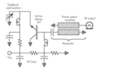
A feedback voltage divider is formed using the intrinsic base-emitter capacitance and a discrete capacitor attached from the emitter to ground. In this configuration, a negative resistance is generated at the collector-base junction to which a resonator may be coupled, and from which power at the resonator frequency may be extracted. Figure 2 illustrates the complete schematic of the grounded-collector oscillator with the discrete inductance replaced with a distributed, coupled transmission line.
2. This is a common-collector, coupled transmission-line resonator oscillator. The common-collector oscillator circuit topology with capacitor-coupled, grounded resonator is fundamental to the push-push oscillator topology.
The series capacitor serves as an effective coupling mechanism to the coupled transmission-line resonator. In addition, the feedback capacitor is illustrated as an adjustable element to highlight the profound influence on oscillator parameters—specifically, power output, phase noise, and start voltage.
The common-collector oscillator using the coupled transmission-line resonator is selected for study because the structure forms an element of the push-push oscillator architecture, as will be demonstrated. The coupled transmission-line resonator facilitates examination of the output power coupling via the odd- and even-mode impedance while observing the dynamic load line and determination of the oscillator frequency and power output.
Loading is introduced to the oscillator system by means of the coupled transmission-line resonator and the series capacitor. This is important for all aspects of oscillator design because high-quality signal generation often has been a matter of accepting the output signal quality from a given configuration. Greater spectral signal quality was attainable only when using high-quality resonators. Recently, this adage has been proven false by MMIC oscillator performance that exhibits phase noise comparable to good quality cavity oscillators at X-band (an example is the HMC398QS MMIC VCO, see datasheet). The ability to accurately simulate the loading effects on power output, phase noise, and harmonics suggests the use of lower cost oscillator circuit implementation.
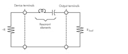
The coupled transmission line facilitates both output loading and control of the total resistance reflected across the collector-base port of the oscillator at the resonant frequency. This effect may be readily understood by observing the equivalent circuit of the coupled transmission line (Fig. 3).
3. Shown is the equivalent circuit of coupled transmission line. This configuration is selected due to the ease with which to observe the effects of load coupling.
The coupled transmission line implements an impedance transformer in which the impedance transformation ratio is controlled by the odd- and even-mode admittance. This is a powerful analysis tool because the load line and the reflected impedance may now be observed over various coupling values. Under very light loading conditions, the common-collector oscillator behaves in a similar manner to that encountered when connected in the push-push configuration.
Steady-State Operation
The “prevailing” wisdom with respect to oscillator operation in the steady-state may be succinctly represented with the graphic in Figure 4. Here, a negative resistance—whether created via feedback or transfer electron device, i.e., Gunn or Impatt diode—is connected to a resonant circuit and then to a load.
4. All oscillators operating in the steady-state, shown here, may be distilled to this circuit embodiment.
Typically, both device and load are coupled to the resonator using either distributed or lumped-element circuit components. In the steady-state, the total loop resistance is equal to zero. Otherwise, the oscillator signal would continue to increase until the device saturates and the negative resistance decreases to the value of the positive resistance of the coupled load. It’s for this reason that the large-signal impedance is examined at the negative resistance port of the common-collector oscillator and the coupling value is adjusted to ensure that the conditions for sustained oscillation are achieved.
If the load coupling is adjusted to the point where the net loop resistance becomes positive, the system will cease to oscillate. In fact, this condition was examined and found to validate the intuitive oscillator operation. The fact that this result was validated by the large-signal simulation of the common-collector oscillator and correlation with earlier experimental results of load coupling was quite satisfying. Hence, the simulation algorithm and model proved to be valid. However, specific transistor model parametric values are still in question.
Footnote
The harmonic-balance simulation software for this task is offered by AWR Microwave Office version 5. The harmonic-balance method is a powerful technique for the analysis of high-frequency, nonlinear circuits such as mixers, power amplifiers, and oscillators. Additional information can be found at www.awrcorp.com.
Author’s Note
This technical memorandum was originally prepared for a M/A-COM engineering conference in 2005 by Kenneth Puglia and Arjang Pakfar. M/A-COM engineering conferences were initiated by Harlan Howe as a venue to share technical information and advance interaction and communications among the technical staff. The M/A-COM engineering conferences also promoted professionalism and encouragement of the engineering staff to further document and formally present at a company sponsored, off-site annual event. The author recently revisited this article series as part of an assessment of software analysis and simulation tools that provide unique opportunities for education, as well as system and circuit intuitive understanding.
References
1. Bender, J. and Wong, C., “Push-Push Design Extends Bipolar Frequency Range,” Microwaves and RF, October 1983.
2. Nativ, Z. and Shur, Y., “Push-Push VCO Design with CAD Tools,” Microwave Journal, February 1989.
3. Gris, M., “Wideband, Low Phase Noise Push-Push Oscillator,” Applied Microwave and Wireless, January 2000.


