This file type includes high resolution graphics and schematics when applicable.
Low-noise amplifiers (LNAs) are essential to many RF/microwave wireless systems, typically employed in receivers to boost low-level signals without adding noise. Although LNA designers and specifiers often think of these amplifiers in terms of their active devices, the choice of printed-circuit-board (PCB) material can play a large role in the ultimate performance achieved from an LNA, with the PCB design typically focused on providing good impedance-matching networks for the active devices, low loss from the active devices to the antenna, and minimal electromagnetic interference (EMI).
A suitable PCB material can also aid an LNA design by minimizing the effects of heat on such amplifier performance parameters as noise figure and gain. All in all, PCB selection can contribute quite a bit to the final performance levels possible from an LNA design.
A number of different PCB material properties should be considered for any LNA “design candidate,” including dielectric constant (Dk or εr), temperature coefficient of Dk, dissipation factor (Df), thermal conductivity, and even substrate thickness tolerance. For example, to achieve the tight impedance matching often needed to maintain low amplifier noise figures, a PCB material’s Dk should be tightly controlled across the material. These impedance-matching networks—and an LNA’s noise figure—can also be affected by a PCB material’s temperature coefficient of dielectric constant (TCDk).
In addition, impedance-matching circuits are impacted by variations in substrate thickness, so tighter substrate thickness tolerances are recommended for LNA designs. Low circuit-material Df and smooth PCB copper surfaces also can help minimize loss from a feed line to an LNA, so as to help maintain low noise figure. Since an LNA’s noise floor can rise with temperature, high PCB thermal conductivity helps to minimize these noise-figure-elevating temperature rises at higher signal levels.
Circuit laminates designed for high-frequency applications usually feature tight control of Dk across the material, but materials can differ in terms of their levels of Dk tolerance. Although most materials provide Dk tolerance within ±10%, materials with tighter Dk tolerance are also available. Ironically, although Dk control and tolerance is often directly related to achieving the impedance-matching networks needed for LNAs, it is often the variations in substrate thickness that have greater impact on achieving tight impedance-matching networks. While variations in thick circuit substrates can have less of an effect on impedance-matching networks, thinner substrates are typically used for minimizing noise in LNA circuits, and the thickness tolerance of these thinner substrates is important for achieving tight impedance matching networks.
Other circuit-material tolerances that can affect impedance-matching circuitry include conductor width tolerances, copper thickness tolerances, and issues associated with circuit fabrication. The weight of such tolerances depends on the particular LNA circuit design. The copper thickness tolerance, for example, has more influence on coupled circuit features such as coplanar circuits while the effects of conductor width on a circuit are related to the substrate thickness: thinner circuits will exhibit more change in impedance for a change in conductor width than thicker circuits.
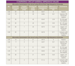
As the table shows, a number of variables can affect the characteristic impedance of a PCB. Comparing the variables in the table reveals that substrate thickness has the most significant effect on the circuit impedance. For many circuit laminates, a thickness variation of ±10% is a realistic value, although high-frequency laminates are available with tighter thickness tolerances.
Another PCB material parameter that can affect the impedance-matching networks needed in LNA designs is the Dk tolerance. The table shows materials with Dk values within 10% of their nominal values, although high-frequency laminates are available with tighter Dk tolerances. Some circuit laminates are available with Dk controlled within ±0.05 of the Dk value which, for a circuit material with Dk of 3.5, translates to a variation within about ±1.4%. Using a material with such tight Dk tolerance minimizes the effect of this material parameter on LNA performance by enabling tight impedance-matching networks
As the table shows, two items specific to PCB fabrication can affect impedance matching and LNA performance. Copper thickness variations of 1 to 2 mils are not unusual, although circuit fabrication with tighter specifications are available. Also, variations in conductor width can also affect impedance matching, and a difference of 1 mil in conductor width is not unusual for different PCBs.
The top and bottom parts of the table compare microstrip circuits fabricated on 20-mil-thick (top) and 10-mil-thick (bottom) substrate materials. The differences in circuit-material thickness are affected differently by the variables, such as copper thickness and conductor width. Basically, the thinner circuits are more sensitive to conductor effects and changes in copper thickness and conductor width.
This file type includes high resolution graphics and schematics when applicable.
Assessing The TCDk
This file type includes high resolution graphics and schematics when applicable.
The TCDk of a PCB material is an important parameter to consider when choosing circuit laminates for LNAs. Especially in applications with changing operating temperatures, in which changes in Dk can affect impedance-matching networks and possible LNA gain and noise figure, TCDk must be compared for candidate materials. It can denote a positive or negative change for a material’s Dk value: For some materials, the Dk will increase with an increase in temperature and, for some, the Dk will decrease with rising temperature. Nearly pure polytetrafluoroethylene (PTFE) circuit materials typically exhibit high TCDk values in the range of 400 ppm/°C. Some PTFE-based circuit materials employ special fillers to minimize TCDk effects. Many high-frequency laminates with high Dk values also possess high TCDk values, although special formulations are available when needed.
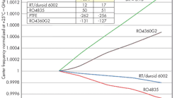
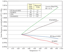
To better understand the effects of PCB material TCDk variations on high-frequency performance, a simple study was undertaken by fabricating edge-coupled microstrip bandpass filters on different laminates. Filters were designed with center frequency of 2.5 GHz, were heated from room temperature to about +200°F, and the resulting shifts in center frequency were monitored. From the shifts, the circuit material Dk values were extrapolated (Fig. 1).
The ceramic-filled PTFE laminate with higher Dk value (6.15) exhibits the greatest difference in TCDk. Improved TCDk behavior is available from the hydrocarbon material having a similar Dk value (the RO4360G2 laminate from Rogers Corp. with Dk of 6.4). The best material in this study is a specially formulated PTFE laminate, with the RO4835 laminate showing very good results.
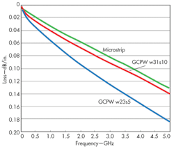
For any PCB design for an LNA, the feed line from the antenna or other input port to the LNA’s active devices should have the lowest loss possible, since additional loss will raise the amplifier’s noise floor. The feed line should also be shielded from outside EMI as well as on-board EM radiation to minimize those sources of noise. To minimize noise, a grounded-coplanar-waveguide (GCPW) transmission line is often used for the feed line instead of lower-loss microstrip transmission line. The GCPW has ground planes near the signal conductor and on the same layer, which can help to minimize added noise on the feed line due to EMI. To compare, Fig. 2 shows transmission-line insertion loss from two GCPW circuits and one microstrip configuration.
As Fig. 2 shows, the microstrip transmission line has the lowest loss. The two GCPW configurations have different ground-signal-ground (GSG) geometries on the signal plane, while both have a solid ground plane below the signal plane. The nomenclature of w31s10 indicates the GSG configuration has a 31-mil-wide signal conductor and 10-mil-wide space between the adjacent ground planes. The w23s5 material is a 23-mil-wide signal conductor with 5-mil spacing to the adjacent ground planes.
The tighter-coupled GCPW (w23s5) circuit is better for minimizing EMI concerns; unfortunately, it is also suffers an increase in conductor loss (and insertion loss). The other GCPW configuration represents a good tradeoff between the microstrip circuit and the tightly coupled GCPW version.
The high-frequency circuit material used in Fig. 2 has a Df of 0.0037 when tested at 10 GHz and is considered a low-loss microwave material. But this same material can achieve improved insertion loss by using a different copper type with a smoother copper surface. The smoother surface yields a lower conductor loss and lower insertion loss. A circuit with lower insertion loss is advantageous for not adding to the noise floor, and there are alternative high-frequency circuit materials with lower Df to be considered.
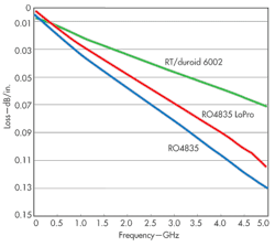
Figure 3 compares microstrip transmission-line circuits using the same thickness but different materials. The red and blue curves are based on the same circuit substrate, although RO4835 LoPro features circuit laminate with smooth copper surface for lower loss. The RT/duroid 6002 circuit material is a very low-loss laminate with Df of 0.0012 at 10 GHz, with smooth copper surface to minimize loss.
Although LNAs are not associated with the need for thermal management in the same manner as power amplifiers (PAs), LNAs can be affected by the generation of heat and its effects on noise performance. Of the different aspects to consider as part of the thermal management of a PCB material, substrate thermal conductivity is one of the key material properties. Most circuit materials are considered a thermal insulator with thermal conductivity values in the range of 0.20 to 0.3 W/m/K. In comparison, copper has a thermal conductivity value of about 400 W/m/K. The difference in value shows why PCB substrates are considered thermal insulators rather than conductors.
However, the heat flow path is very often through the PCB substrate, in which case the substrate is acting like a thermal conductor (with poor thermal conductivity properties). Any significant increase in substrate thermal conductivity can improve the heat flow in the PCB and allow the circuit to remain cooler, assuming it is attached to a heat sink or some other cooling mechanism.
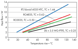
To understand the importance of thermal conductivity (TC), a study was performed on the heat flow of a 20-mil-thick microstrip circuit fabricated on different high-frequency circuit materials. Figure 4 plots the TC values for the different materials, with the material having the best thermal conductivity (TC = 1.44 W/m/K) exhibiting the highest heat flow. High heat flow helps keep a circuit cooler and minimize thermal effects on amplifier noise figure.
The WG-PTFE material in Fig. 4 has a thermal conductivity which is about the average in the high-frequency circuit material industry. Materials with thermal conductivity in the range of 0.50 to 0.62 W/m/K are considered quite good; a circuit material with a value of 1.44 W/m/K is considered exceptionally good.
Circuit-material properties can have an impact on the performance of an LNA. In general, LNA applications are sensitive to impedance differences, due to critical impedance-matching networks which are necessary to tune the circuit to optimum performance. Circuit-material TCDk performance is important, since it is an indication of how Dk—and impedance—will change with temperature. Insertion loss is yet another important material parameter which can affect LNA noise figure. And thermal management is critical, since thermal effects can also influence LNA noise-figure performance.
In short, some circuit materials are better suited than others for LNAs. An ideal circuit material for an RF/microwave LNA should provide tight control of Dk, small thickness variation, low loss, and outstanding thermal conductivity.
John Coonrod, Senior Market Development Engineer
Rogers Corp., Advanced Circuit Materials Div., 100 S. Roosevelt Ave., Chandler, AZ 85226-3416; (480) 961-1382
This file type includes high resolution graphics and schematics when applicable.
