This file type includes high resolution graphics and schematics when applicable.
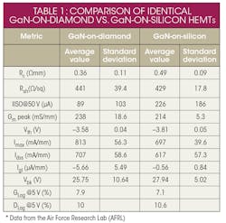
Solid-state power amplifiers (PAs) continually push the boundaries on power density in ever-smaller package sizes. Though that’s desirable from a cost, size, and weight perspective, the thermal energy for gallium-nitride (GaN)-based devices operating at high power levels is magnitudes greater than prior technologies. Such thermal-energy density in and around these devices significantly strains the transistors and surrounding components. Therefore, to get the most out of these new materials, GaN and passive-device manufacturers are now turning to diamond substrates as a next-generation material (Table 1).
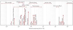
Diamond maintains the highest thermal conductivity of any material at room temperature (Fig. 1). Alongside its extreme hardness and optical transmittance, these characteristics make diamond a highly attractive material for power electronics. High-performance RF amplifiers and laser-diode devices are the two main applications for diamond materials. For RF applications, the primary interest surrounds telecommunications and electronic-warfare (EW) amplifiers and passives.
However, natural diamonds and high-pressure high-temperature (HPHT) synthetic diamonds aren’t suited for electronics manufacturing. In this industry, the dominant form of diamond is the chemical-vapor-deposition (CVD) diamond.
How is CVD Diamond Made?
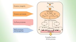
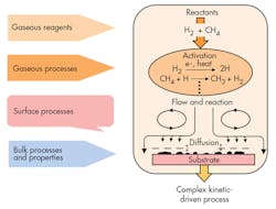
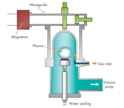
Creating a material that’s produced through application of the Earth’s heat and pressure over millions of years doesn’t come easily or cheaply. Either those extreme conditions have to be replicated, or it requires the use of clever physics and chemistry. The CVD diamond process does that the latter. Using carbon dioxide, methane, and high-energy microwave plasma, a molecule-by-molecule construction of a diamond wafer is possible (Fig. 2).
“There are several inputs that have to be controlled carefully to achieve the highest purity diamond. Those inputs are power, pressure, gas selection, and the temperature of the substrate the diamond is grown on,” says Bruce Bolliger, Head of Sales And Marketing for Element Six. These control parameters can influence the properties of the diamond to a high degree. Bolliger continues, “This includes engineering imperfections, thermal grade, and different optical characteristics. As the process grows the diamond material molecule by molecule, the process allows for very refined control.”
Most of the diamond material for RF applications is polycrystalline, and it’s targeted mainly for thermal applications (Fig. 3). Single-crystal diamond, predominantly used for its optical properties, has higher thermal conductivity than polycrystalline—roughly 3000 W/mK compared to 2000 W/mK. But the increased cost and limited 8- by 8-mm size reduces its viability for RF applications.
Diamond growth rate determines the grain size of the polycrystalline diamond. If the CVD diamond is grown more slowly, the diamond will have a larger grain size, which is typically a higher-performing material. For example, a 1000-W/mK quality CVD diamond is basically half the cost of a 2000-W/mK diamond, as its growth time is roughly half the time of the lower-quality diamond. In general, the variable growth rate enables quality control over the diamond substrate.
Diamond in Optics
Optically, diamond can be transmitted over a very broad range of frequencies, including infrared (IR). For applications with high-powered lasers, a lens must be able to handle lots of power without changing shape or expanding. CVD diamond is well-suited to this application as well as others. However, high costs and a lack of mainstream applications may hinder diamond research.
In addition, the polycrystalline diamond method can produce larger wafers that are at most 140 mm in diameter and 2 mm thick. For thermal applications, substrate thickness typically measures between 300 and 500 µm. Post-processing polishing and cutting can form the diamond into different grades and sizes, depending on the application.
Using CVD Diamond as Heat Spreaders
For RF technologies, CVD diamond’s first main application has been to act as a heat spreader. The heat spreader is inserted between the RF die and the substrate to channel the thermal conduction away from the die material (Fig. 4). “Good thermal transfer demands that the interface between the die and the diamond be as thermally optimal as possible,” says Bolliger. “If this interface is fabricated incorrectly, the diamond heat spreader is ineffective.”
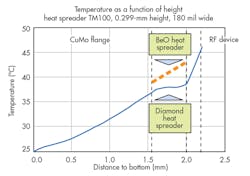
Poor interface characteristics can reduce the thermal conduction gain of any heat spreader material. With diamond, however, any loss of thermal transfer is dramatic compared to the benefits (Fig. 5). Bolliger continues, “If done right, the diamond heat spreader could reduce the thermal resistance by 25-30%. We recommend keeping the solder layer between the heat spreader and die as thin as possible to minimize its degradation of the thermal conductivity of the stack.”
A metallization step helps with the interface characteristics between the die and the diamond heat spreader. Generally, it entails layers of titanium, platinum, and gold. Platinum is used because a few metals will adhere well to titanium—a thin layer of titanium is sputtered on followed by platinum. The platinum also prevents the die material from bonding to the titanium. A layer of gold is deposited on top to help with adhesion as the wire bonds are attached during soldering
“BeO [beryllium oxide] is a good heat spreader, but has a thermal conductivity as much as 10 times lower than CVD diamond,” says Bolliger. “Diamond doesn’t collect any heat within the material itself, and so its thermal transfer is extremely rapid.” With polycrystalline diamond, the larger crystals enable more rapid phonon thermal transfer through the material. He continues, “For example, comparing the TM100 (1000-W/mK thermal conductivity with smaller crystals) CVD diamond at 0.3 mm compared to BeO led to a 30% reduction in thermal resistance.”
GaN-On-Diamond Could Reduce Thermal Noise
CVD diamond substrates can dramatically reduce the thermal energy near signal-conditioning and amplifying transistors. This reduction, in turn, may significantly lower a signal’s thermal noise. Applications from telecommunications to EW and SIGINT can benefit from high-powered, low-noise devices. For example, the amount of noise introduced by power amplifiers limits the latest modulation techniques at high constellation levels. This burden is usually borne by the receivers. In addition, there’s demand for low-noise amplifiers (LNAs) that can handle a wide range of voltages, powers, and frequencies.
There are diminishing returns with using ever higher quality CVD diamond, though. Once the thermal conduction can remove most of the heat, less benefit can be attained by using higher grades. Bolliger says, “With the same comparison with BeO using TM180 (1800 W/mK thermal conductivity), we only experienced a 37% improvement.”
Diamond as a heat spreader does aid the thermal transfer. Yet, the further away the diamond material is from the die, the less likely it is to increase thermal conduction. When using a heat spreader, the diamond is still separated from the die substrate by 100 to 300 µm. Having the diamond within a micron of the heat source can reduce thermal resistance by as much as 50%.
How is GaN-on-Diamond Made?
Using a diamond substrate will ensure that the GaN and diamond are as close as possible. Though no process exists to grow GaN directly on top of CVD diamond, a specialized process has been developed. Bolliger explains, “The work of developing GaN-on-diamond technology has been going on for about 10 years. I would say many years of which have been spent on optimizing the interface between the materials.”
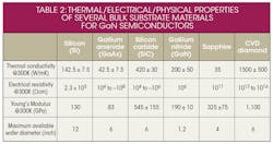
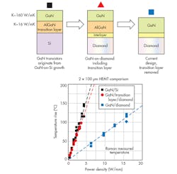
Initially, GaN is grown on a silicon wafer, but the silicon is later etched away (Table 2). The transition layers added to the GaN are etched away prior to the deposition of an interface layer on the GaN (Fig. 6). Next, diamond is grown on the interface layer. That interface layer is one of the most critical aspects of the process, as its quality can dramatically diminish the benefits of a diamond substrate (Fig. 7).
GaN-on-Diamond Justification
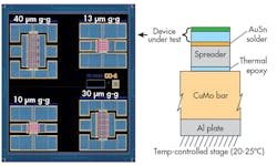
Diamonds offer lots of promise for GaN PAs. Although the PAs create very small hotspots, diamond spreads heat equally in all three dimensions. Thus, for a very small hotspot, diamonds are particularly effective. Companies like Raytheon and TriQuint (now Qorvo), with funding from DARPA, have researched the potential benefits of diamond substrates (Fig. 8).
“Raytheon demonstrated that the space between the GaN-on-diamond gates can be reduced by as much as 4X, with the device running at comparable temperatures as with GaN-on-SiC materials,” says Bolliger. Reducing the thermal resistance near the transistors of a PA can provide headroom to reduce the overall device size. Bolliger continues, “Also, the peak power and peak temperature are nearly the same. The enhanced thermal conductivity led to certainly more than a three times increase in power density.”
Several advantages to GaN-on-diamond outweigh some of the initial cost considerations. For instance, the watts-per-meter of wafer space is much lower with a diamond substrate. The smaller chip leads to much less in handling costs, and could translate to smaller device sizes. Overall, higher performance in a smaller space could substantially lower system costs.
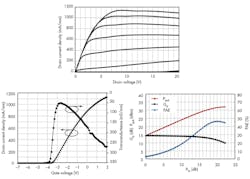
“As TriQuint’s tests of RF performance of GaN-on-diamond to GaN-on-SiC show, GaN-on-diamond doesn’t require a sacrifice in performance,” says Bolliger. In addition, diamond negligibly changes shape under a wide thermal range, which benefits optical applications (Fig. 9). This lack of thermal expansion and contraction cycles could reduce device wear. Bolliger adds, “Secondly, in dc reliability tests compared with GaN-on-Si, we ran devices from both materials for many hours at 200ºC. Neither the GaN-on-Si nor the GaN-on-diamond devices failed, so we cranked up the temperature to 350ºC and the GaN-on-diamond devices still ran strong for over 1000 hours, while the GaN-on-Si devices began to degrade over the same time period.”
The benefit of lowering a device’s thermal resistance is that manufacturers can choose between a few optional enhancements. For example, they can run devices at lower temperatures and double their lifetime. Or, they can run the devices at higher power and at the same temperature. Device manufacturers can even run the device hotter, at similar lifetimes, and spend less on device cooling costs.
Because the hydrogen and methane gases are relatively inexpensive, only two main costs are incurred when creating CVD diamonds. The most significant costs lie in the equipment and energy used to strip the carbons from the gases. The plasma reactors need very consistent power over the hours and days it may take to grow a diamond wafer. Few locations have the electrical infrastructure to support such an operation. Growing large amounts of diamond material requires multiple reactors, so the costs scale linearly with the demand of CVD diamond.
CVD Diamond Meets Resistives
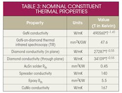
Like GaN PAs, high-power and high-frequency resistives are limited by thermal challenges. For resistors and attenuators, most of the energy lost is dissipated as heat. Removing this heat typically increases the size, weight, and cost of the resistive, as well as the surrounding assembly (Table 3).
”Over the last decade, we came to realize that RF passive component technology has matured significantly,” says Kai Loh, Senior Product manager for EMC Technologies and Florida RF Labs. “Though there are techniques for enhancing component performance in certain bands, the manufacturing techniques are mostly matured.”
To avoid being the limiting factor, however, resistives have to keep pace with the performance of other components in an RF assembly. In response, Loh says, “We came to the conclusion that innovation would have to come through materials. As we analyzed material options, we came to CVD diamond as the ideal platform for next-generation resistives.”
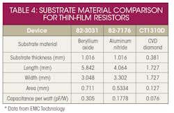
Although conventional materials may be cheaper, CVD diamond has roughly 6X higher thermal conductivity than beryllium oxide (BeO) (Table 4). In addition, it outperforms aluminum nitride (AlN) by about 7X or 8X. Conventional materials cannot conduct heat away quickly enough, which usually leads to a thermal bottleneck. Thermal conduction away from the part is also crucial for the part’s operational lifetime and reliability.
A resistor’s power-handling capability depends on size. “A 0.25- by 0.25-in. resistor using traditional materials can be shrunk to a 1310 diamond chip capable of handling 150 W,” says Loh. Using CVD diamond, the size of a resistive chip can be reduced. Loh adds, “To make a resistor that can handle 300 W would take a 0.375-by-0.375 footprint. There is a 2010 resistor chip made with CVD diamond that can handle 300 W.”
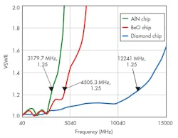
CVD diamond also helps enhance the electrical performance of resistives. The dielectric constant of a CVD diamond is much lower than other materials, which reduces the parasitic capacitance (Fig. 10). For thin-film resistors, this leads to higher-frequency operation.
Another benefit of smaller resistive components is their decreased susceptibility to CTE mismatch issues. The hardness and tensile strength of diamond reduces the likelihood of cracking or fracturing under high CTE mismatch stresses.
The combination of small size and higher-frequency performance opens up opportunities for satellite-communications and telecommunications applications, such as point-to-point radio and backhaul. In addition, diamond resistives are seeing increased adoption in weight- and space-constrained applications. Examples include phased-array radars, Wilkinson power dividers, and combiners, which require many resistives (thus increasing both weight and volume). However, space applications might be the most weight- and volume-critical, where an estimated $10,000 to $100,000 is paid per pound of payload.
Diamond as a Semiconductor
When considering CVD diamond’s impressive properties as a substrate, one wonders how it could be used as a semiconductor. Research into development of synthetic diamond as a semiconductor material revealed it to have a very wide bandgap and very low parasitics. Its other material benefits all point to diamond’s potential as a high-performing semiconductor. Due to a lack of applications and high cost, however, few organizations are working on advancing the material for future use.
“At higher volumes, there is roughly a 30% cost difference between diamond and conventional passives,” says Loh. “Though more expensive initially, in practical applications there is an opportunity to realize reduced resistive real estate and reduce the envelope size of the system.” Potentially, these reductions could lead to value that is beyond what would be saved in the up-front cost of materials. Loh continues, “Additionally, the 30% figure is comparing standard components to standard components. If high reliability or space testing is involved, the screening costs are the same.”
In summary, using CVD diamond as a heat spreader or substrate for active components and resistives has tremendous performance-enhancing potential in terms of increased power density, decreased size/weight, or higher reliability. Though the cost of CVD diamond may limit the material’s penetration into many high-volume, low-cost markets, reasonable justifications can be made for those added system-level costs in high-performance markets. Further research and development could eventually lead to lower-cost CVD diamonds and even diamond-as-semiconductor. Undoubtedly, the diamond’s footprint will continue to grow in high-performance RF applications.
This file type includes high resolution graphics and schematics when applicable.
Resources:
CVD Diamond Delivers A Cool Competitive Advantage
AlGaN/GaN HEMTs on diamond substrate with over 7W/mm output power density at 10 GHz
Diamond RF Resistives: The Answer To High Power and Low Capacitance
CVD Diamond High Power Resistors and Terminations
Analysis and Characterization of Thermal Transport in GaN HEMTs on Diamond Substrates
