Miniaturization of handsets and other wireless devices creates scores of shielding challenges as high-frequency components become more closely spaced. As printed-circuit boards (PCBs) shrink, new electromagnetic-interference (EMI) shielding solutions must provide greater levels of interference suppression, but without significantly adding mass, weight, and cost to a device. Fortunately, a new shielding technology developed by W.L. Gore & Associates called snapSHOT™ shield, replaces bulkier soldered approaches with a snap-on metallized thermoformed shell that can be attached to a PCB by means of standard ball-grid-array (BGA) solder spheres.
In understanding the shielding requirements of compact wireless designs, the shortcomings of traditional test methods (mostly based on military requirements) become apparent when applied to battery-powered portable wireless designs. Some test methods, such as ASTM D 49351 for planar shielding and a coaxial cell2 for EMI gaskets, for example were developed to characterize the materials that would ultimately comprise an EMI enclosure. But there remain no formal published test methods to evaluate the shielding effectiveness (SE) of a shield assembled to the PCB of a portable wireless device.
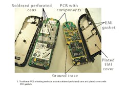
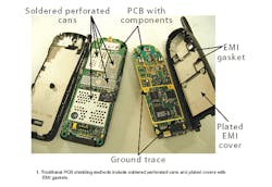
At present, two primary shielding approaches are used in cellular telephones: soldered perforated cans and plated covers with EMI gaskets (Fig. 1).
Both try to create a complete shield around the PCB's components to ensure proper electrical performance and comply with regulatory requirements for EMI emissions and susceptance.
The goal of an EMI shield is to create a Faraday cage around the enclosed RF components using the six sides of a metallic box. The top five sides are created using a shielding cover or metal can, while the bottom side is achieved by using the ground plane within the PCB. In an ideal enclosure, no emissions would enter or exit the box. In reality, leaks do occur, such as from holes perforated into soldered cans that allow thermal heat transfer during solder reflow. Leaks can also occur from imperfections along an EMI gasket or solder attachments. Leaks are also possible from the spaces between ground viaholes used to electrically connect the shielding cover to the ground plane.
Shields designed for portable devices must be light in weight and low in cost, but they must also meet demanding mechanical and electrical requirements. Phenomenon such as cavity resonance, aperture radiation, and planar shielding are factors RF engineers face when designing shielding enclosures. The problem is further complicated by the fact that accurate EM field prediction from complicated PCB assemblies, particularly in the near field, is virtually impossible, forcing many engineers to build custom test fixtures to evaluate their designs.
To create the Faraday cage required for proper shielding, a metallic enclosure must be placed around and in close proximity to the components on a PCB. Unfortunately, this may have adverse effects on the performance of the components and the functionality of the circuit, with the greatest concern being enclosure (cavity) resonances at any of the PCB's operating frequencies. To study this, a simple test fixture was designed to mimic the effect of placing a metallic enclosure over RF components.
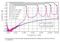
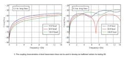
The test fixture (Fig. 2) consists of two 50-Ω, 0805 resistors that are launched from SMA connectors from the opposite side of the ground plane. The spacing is arbitrarily set at 0.5 in. (1.27 cm) so that minimal coupling would occur between the two components when the shield is not in place (Fig. 3).
Coupling was determined from 20logS21 measurements on a microwave vector network analyzer (VNA). A perforated metal square can, with inside dimensions of 1.805 × 0.114 in. (4.584 × 0.29 cm), was soldered over the components to illustrate the effects of a metal cavity. The simple formula in Fig. 3 was used to roughly calculate the resonant modes of the EMI enclosure. The formula applies to rectangular cavities and is fairly accurate if the cavity is filled with air. However, most enclosures on PCBs will include the PCB material and components within them, raising the cavity's effective dielectric constant and thus lowering its resonant frequency.
With the shield in place, coupling between the two components is severely increased at and around the resonances, as much as 50 dB for this fixture. Peaks occur at the resonant frequencies calculated by the formula. Below the first resonant frequency, the coupling between the two components is virtually unchanged. Thus, it is critical to consider these resonant conditions when designing EMI enclosures.
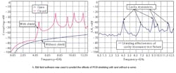
A more accurate way to predict the effects of a rectangular cavity involves the use of an EM field simulator, such as the Sonnet® Professional Planar Software Suite from Sonnet Software (Liverpool, NY). This software models planar circuits within a metallic box, and can easily be used to examine the effects of cavity dimensions, substrate material, and metal wall conductivity. (A free version of the software is available on Sonnet's website at www.sonnetusa.com.) Figure 4 shows the response of a model produced by the software, with close agreement to the actual measured data.
Page Title
Another important consideration concerning cavity resonance is the effect on the shielding performance of the enclosure. Since energy inside the cavity is amplified at the resonant modes, it is likely that the shielding effectiveness (SE) would be lowest at these frequencies. As Fig. 4 shows, the SE drops significantly at each cavity resonance (due to the dimensions of the cavity).
The methods for evaluating the effectiveness of PCB shields can be broken into three categories: compliance testing, functional testing, and indirect testing. Compliance testing involves evaluation of the final product given industry-standard test methods and acceptance levels, such as spurious emissions, susceptibility, or electrostatic discharge (ESD). Functional testing involves evaluation according to performance requirements set by the manufacturer. Intercavity shielding, radiation from the antenna back into the receiver (Rx), and phase noise are examples of parameters that would be considered.
The last category, indirect testing, is used when describing shielding products. Methods such MIL G 83528B, ASTM D 4935, and ASTM D 991 are guidelines followed by shielding manufacturers to evaluate their products. These methods can characterize the constituent properties of a shield, but cannot predict the performance in a specific application.
Typical surface-mount-technology (SMT) components suffer minimal levels of radiation, although these levels are not negligible. Predicting the radiation response, particularly in the near field, of typical SMT devices is a formidable task. A first step is to consider the coupling between two microstrip lines that would be used to connect components on the PCB. Short transmission lines, even when close together, exhibit very little coupling. This characteristic can help to develop an inefficient radiator that can be used as a test vehicle (Fig. 5).
Since the dielectric substrate thickness on the outer layers of the PCB is usually very thin, it is desirable to have the radiating element be a separate component, instead of integrating it onto the PCB. The height of a separate radiator can be readily adjusted, while maintaining the height sufficiently lower than the inside height of the shield. By using the remaining dimensions of the transmission-line radiating element (height, length, width, and termination impedance), the response of the radiator can be optimized for testing shields on PCBs.
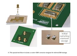
The special test fixture developed for testing shields on PCBs (Fig. 6) includes a custom-designed SMA connector that, using a solder pre-form, completely seals the launch point to the ground plane of the PCB.
The connectors then feed the radiating elements that are attached to the opposite side of the PCB. The shields would then be centered and attached over each of the elements.
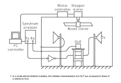
The mode-stirred reverberation chamber technique (Fig. 7) is an excellent EMI test method because of its high dynamic range and repeatability.4,5 In this technique, the radiation characteristic from the device under test (DUT) is compared to that of a reference horn antenna. Measurements are first performed on the horn antenna, then the DUT is substituted for the horn and tested. Of course, only one radiator/cavity can be tested at a time. The radiator is first measured without a shield over it, then the shield is attached and the device is re-measured. The SE is calculated as the difference between the received power levels (in decibels) before and after the shield is applied.
The frequency range of such a test is determined by the room dimensions, the test equipment, and the antenna bandwidth. The main limitation is usually the lower frequency boundary, determined by the room size and antenna used. A frequency range of 1 to 13 GHz was used for the tests in this article.
Practically, EMI enclosure cannot be made to be a complete Faraday shield. Gaps due to perforations in the shields, incomplete shields, breaks in the shielding gasket, spaces between grounding vias, and relief areas in the ground plane are necessary to manufacture the complete PCB. But as long as the size of the aperture is much smaller than the wavelength of the highest frequency of interest, it should not cause an appreciable amount of leakage.
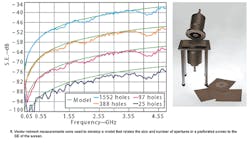
The effects of apertures much smaller than a wavelength at the highest operating frequency of interest has been studied to great lengths.9-11 For perforated screens, the formula of Fig. 8 has been used to show the frequency relationship between the size of the aperture and SE. Although this frequency dependence represents an accurate relationship for the far-field response of a large array of holes, an offset factor in SE can deviate quite a bit from real-life applications. To overcome this, a relationship for the far-field (plane-wave) response was derived using empirical data taken from thin copper sheets perforated using the traditional hexagonal pattern. Initially, 1-mm-diameter holes were placed on a 1.7-mm hexagonal grid, such that about 1552 holes fell within the annulus of a typical ASTM D 4935 test cell. The SE was obtained using S21 measurements with and without the sheets in place (Fig. 8).
A simple model was generated to represent this test pattern, using the formula of Fig. 8 and a correction offset factor. The next three test patterns were generated by doubling the spacing between the holes each time. This way, about four times fewer holes fell within the annulus of the coaxial cell for each pattern. To generate the modeled data, the original model was changed by a factor of 4 each time, which yielded 12-dB offsets. As Fig. 8 shows, the frequency relationship follows what would be expected for plane-wave excitation of perforated thin sheets.
Page Title
The next logical step is to see how a perforated soldered can would perform using the same 1-mm hole size on a 1.7-mm grid. Using the test method described earlier, a 16.3 × 22.5 × 3.1-mm can, completely soldered around its perimeter, was used as the shield. Using the model generated from the plane-wave experiment, a prediction was made for (127) 1-mm holes (Fig. 9).
The surprising result of an overall lower SE is added to the fact that the response is flat with frequency, even at low frequencies. This shows that even at low frequencies, where the size of the apertures are extremely small compared to the wavelength, the SE remains unchanged. Cooperative research with the University of Delaware, using custom method of moment software, has confirmed these results (and will be published formally at the 2003 IEEE EMC symposium in Boston, MA). If the aperture spacing is increased by a factor of 2, thus reducing the total number of holes by a factor of 4, the SE is increased, or shifted by about 12 dB, the same as the plane-wave case.
Perforations in cans allow for heat transfer during solder reflow. Since these cans are attached to a PCB by the same SMT assembly process used for the components, the solder reflow of the components under and around the shields should not be impeded by the can. In typical applications, hexagonal arrays of sufficiently sized holes are placed over the full top surface of a can. A 1.4-mm or larger hole is typical with the hexagonal grid yielding a hole spacing of 4.4 mm and smaller.
To simplify the addition of shielding to PCBs, Gore has developed the "snap-on" snapSHOT shield,™ which consists of a metallized thermoformed shell that is attached to a PCB using standard BGA solder spheres. This approach provides an excellent mechanical and electrical connection and yet allow the user to easily remove the can to get access to the components within the shield. This patented technology (US patent No. 6,377,475; other US and foreign patents pending) offers a PCB-level shield that can be easily attached to a populated board after it has gone through the solder reflow process.
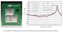
The shield is metallized on the outside with an insulator on the inside. The BGA spheres snap through holes in the shield, creating a robust electrical and mechanical connection to the PCB. The periodicity of the sphere placement is determined by the required shielding performance. Since the inside surface is not conductive, any components that may come in contact with this surface will not be electrically shorted. The snapSHOT™ shield provides significantly improved shielding over similar perforated solder cans with a great deal of design flexibility (Fig. 10).
REFERENCES
- "Standard Test Method for Measuring the Electromagnetic Shielding Effectiveness of Planar Materials," ASTM D 4935, ASTM, Philadelphia, PA.
- Thomas Clupper and Joseph Wheeler, "The effects of gaps introduced into a continuous EMI gasket," ITEM Magazine 2000, Robar Industries, West Conshohocken, PA, 2000.
- Thomas Clupper, "Effects of Apertures in Multiple EMI Enclosures on RF Printed Circuit Boards," Workshop W8, 2001 IEEE EMC Symposium, Montreal, Canada.
- M.L. Crawford and Koepke, "Technical Note 1092: Design, Evaluation, and Use of a Reverberation Chamber for Performing Electromagnetic Susceptibility/Vulnerability Measurements," United States National Bureau of Standards, 1986.
- Ladbury, Koepke, and Cammell, "Technical Note 1508: Evaluation of the NASA Langley Research Center Mode-Stirred Chamber Facility," United States National Institute of Standards and Technology, January 1999.
- Thomas Clupper, "Correlating DC resistance to the shielding effectiveness of an EMI gasket," ITEM Magazine 1999, Robar Industries, West Conshohocken, PA, 1999.
- Foster, Rich, Nobbs, Stiffler, Tozlowski, and Ventura, "EMI Shielding Test Method for small wireless devices," Proceedings of the IMPAS/SMTA Conference, May 2002.
- Ramo, Whinnery, and Van Duzer, Fields and Waves in Communications Electronics, 2nd ed., Wiley, New York, 1984.
- Donald White and Michel Mardiguian, Electronic Shielding, Vol. 3, Interference Control Technologies, Gainesville, VA, 1988.
- Mark Montrose, EMC and the Printed Circuit Board, IEEE, New York, NY, 1999.
- David Weston, Electromagnetic Compatibility: Principles and Applications, 2nd ed., Marcel Dekker, New York, NY.
This file type includes high resolution graphics and schematics when applicable.
This file type includes high resolution graphics and schematics when applicable.
