This file type includes high resolution graphics and schematics.
Cold temperatures can mean minimal signal losses with superconducting circuits. With digital superconductor specialist HYPRES, Inc., those circuits are now available from a new six-layer planarized process that offers a higher integration level of Josephson junction superconducting integrated circuits (ICs). The new fabrication process supports higher current densities on superconducting ICs for energy-efficient solutions in a wide range of applications, including for high-speed computers, advanced wireless communications systems, medical imaging systems, and test and measurement systems. HYPRES is extending the new process in support of its many high-performance standard solutions as well as for the most demanding custom requirements.
Related Articles
• IC Simplifies Receiver Design
• Transceiver ICs Arm Backhaul Radios
• Radio IC Drives LTE Pico Cells
Oleg Mukhanov, Ph.D. is Chief Technology Officer at HYPRES. He is also the co-inventor of Rapid Single Flux Quantum (RSFQ) logic, in which binary bits are encoded in the form of individual magnetic flux quanta. “This is an exciting milestone for HYPRES, its customers, and the superconductor electronics community,” says Mukhanov. “Next-generation superconductor circuit development requires commercially available fabrication processes well beyond today’s four metal layers and critical current densities. We have made six planarized layers—and soon, more—and various increased critical current densities available as part of our commercial foundry services. We made our first customer delivery earlier this year and have new orders in process.”
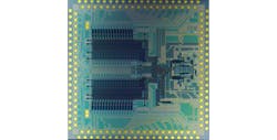
Of course, HYPRES has already accomplished a great deal using as many as four layers of its existing niobium-based superconducting process—including the high-speed digital circuits that make the company attractive for so many different commercial, medical, and military applications. The firm has fabricated high-resolution analog-to-digital converters (ADCs) capable of 100-dB spurious-free dynamic range (SFDR) while operating at clock rates over 30 GHz, as well as a 20 GHz 8-b Arithmetic Logic Unit (ALU) and multichip modules communicating at speeds past 50 Gb/s (Fig. 1).
1. HYPRES has already demonstrated a host of high-speed ADCs capable of 100-dB SFDR performance at clock rates over 30 GHz.
The additional layers, using the company’s proven niobium on silicon 150-mm wafers and sub-1-μm minimum feature size, enable higher circuit density and increased functionality on a chip. Essentially, this makes possible greater circuit complexity in a vertical direction on the superconducting ICs.
These niobium-based superconducting circuits employ Josephson junctions rather than transistors as active devices. A Josephson junction consists of two superconducting metal layers separated by a weak link—usually some form of an insulator tunnel barrier. It was named after British physicist Brian Josephson (1973 Nobel Prize laureate), who predicted the mathematical relationships for the current and voltage across the weak link.
The junction enables direct conduction of electron pairs between the two superconducting layers. Among its other capabilities, a Josephson junction can act as a perfect voltage-to-frequency converter. It can support the flow of current through the junction without an applied voltage.
Already recognized for the design and fabrication of high-speed ICs—such as ADCs and digital signal processing (DSP) circuits for a variety of systems-level and instrumentation applications—HYPRES has used its existing four-niobium-layer fabrication capabilities to produce high-volume circuits, typically with six weeks’ turnaround time. Circuit layouts are generally received at HYPRES in GDS II format for mask preparation, and digital and mixed-signal circuits with as many as 12,000 Josephson junctions have been fabricated with the four-layer process.
HYPRES analog ICs, such as commercial voltage standard circuits, are being produced with 23,000 Josephson junctions. The high-quality circuit fabrication is supported by Class-100 clean rooms and proprietary software simulation tools, in addition to the use of industry-standard software simulation tools.
This file type includes high resolution graphics and schematics.
Strength In Layers
This file type includes high resolution graphics and schematics.
Examples of the company’s product performance capabilities include devices in the Digital-RF™ family, such as the advanced digital receiver (ADR) which provides direct high-speed digitization of RF signals and improved sensitivity and interference handling compared to room-temperature RF/microwave receiver electronics. These receivers are used for a variety of satellite communications (satcom) tasks and signal intelligence applications. The company’s Digital-RF™ receivers operate with broadband digitization at RF/microwave frequencies for multiband, multichannel operation, including 100-dB spurious-free dynamic range (SFDR) for improving performance in satcom systems.
Essential capabilities today include direct digitization at frequencies up to 20 GHz. The superconductor technology has enabled DSP components at clock rates exceeding 100 GHz. The technology helps maintain spectrally pure signals throughout digitization through the use of high-speed clock rates, with low noise and high sensitivity.
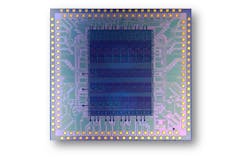
Several years ago, in collaboration with Stony Brook University, HYPRES demonstrated the world’s fastest arithmetic logic unit (ALU), an 8-b, 20-GHz circuit fabricated using HYPRES standard four layer niobium based process (Fig. 2). Admittedly, superconducting circuits require special attention to packaging and maintaining the cryogenic temperature of operation. But companies such as HYPRES have shown for many applications that digital superconducting technology offers excellent performance—especially for functions (such as in ADCs and DSPs) where existing room-temperature electronics technologies (like silicon CMOS) may be reaching practical limits. HYPRES has developed its superconducting technology based on its four-layer fabrication processes, in the production of energy-efficient, high-performance digital circuits for high-speed computing applications.
2. This 8-b, 20-GHz arithmetic logic unit (ALU) was designed on the niobium-based superconducting process in collaboration with Stony Brook University.
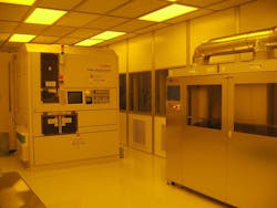
The new six-layer (and beyond) fabrication process has been developed over several years, built with many new processes and techniques included in provisional patent application Rapid Integrated Planarized Process for Layer Extension (RIPPLE). The new fabrication process is made possible with the addition of new hardware and software, including a new lithography stepper system from Canon. This 5X reduction stepper offers fabrication of features as fine as 250 nm, and it boasts the flexibility and versatility needed to support even exotic custom device requirements.
3. The new six-layer superconducting circuit process is made possible with a 5X reduction stepper system from Canon which can fabricate device features as fine as 250 nm.
According to Daniel Yohannes, Ph.D., Director of Fabrication Operations at HYPRES, the new fabrication process brings not only added density, but performance as well. “Our new fabrication process is rapid—approximately 20% faster per layer—and is easily integrated with our current device designs by adding two new layers under the ground plane,” he says. “It is performed with one chemical mechanical polishing planarization step per layer. Moreover, the process is extensible beyond the current six layers, paving the way for a soon-to-be-announced five-year, multi-layer roadmap the company will pursue.” The process has already been extensively exercised and evaluated, with Stanford University becoming the first customer taking delivery from the six-layer process earlier this year.
This file type includes high resolution graphics and schematics.
Assessing The Difference
This file type includes high resolution graphics and schematics.
During a recent company visit with HYPRES Chief Executive Officer Richard Hitt, the difference in integration level with the new process became apparent: from digital circuits with as many as 12,000 Josephson junctions fabricated with the legacy four-layer process to circuits with more than 75,000 Josephson junctions now possible with the new six-layer process. “We needed to put more Josephson junctions on our chips,” notes Hitt, “but with the four-layer process, we were quickly exhausting our capabilities.”
The dividends of more wiring levels available in the new six-layer process will be compounded by the increase in critical current density or Jc - the key parameter defining the switching speed of Josephson junctions. HYPRES legacy four-layer process has typical critical current density of 4.5 kA/cm2. The new process is showing the capability to reach Jc levels of 10, 20 kA/cm2 or greater.
Perhaps more importantly, the new process supports fabrication of superconducting wafers with multiple Jc levels, so that ICs can be further optimized for required functionality. As Hitt points out, “We have unveiled six layers, but we plan to go beyond and do more layers down the road. A greater number of layers translates into greater functional complexity.”
Many customers for superconducting circuits are interested in increased dynamic range of RF receivers, whether in the commercial or military sectors, in order to find and isolate a desired signal amidst a large amount of interference. The superconducting circuits have been proven to provide high dynamic range in wide bandwidth. “We were stuck at four layers for quite some time,” Hitt recalls, “and the four-layer process required that we use thicker and thicker material, with the stress increasing with the thicker layers.” A critical point in creating the new six-layer superconducting process was developing planarization steps that could support reliable viaholes and throughholes between the multiple layers.
The new process is based on pure niobium, rather than on niobium alloy materials. “We started with a planarization technique developed in Japan where we etch back on the metal on a chip before each chemical mechanical planarization step,” Mukhanov says. “They do it layer by layer, where we have developed it further by doing this as a kind of ripple process. We don’t want to have pattern-dependent polishing rates, but want to achieve a more uniform polishing of patterns on the chip.”
Mukhanov mentions that the company is also experimenting with some new materials, notably for the development of high-speed ferromagnetic memory for direct integration with their digital and DSP circuits.
Related Articles
• IC Simplifies Receiver Design
• Transceiver ICs Arm Backhaul Radios
• Radio IC Drives LTE Pico Cells
Superconducting technology is not for everyone, since it requires maintaining the required (cooler) operating conditions, and thus is not suitable for handheld units. But the company is quite supportive of those wishing to design superconductive circuits and provides its design rules for download on the HYPRES website.
In support of its new fabrication capabilities, HYPRES features a full suite of software design tools, including XIC from Whiteley Research and AutoCAD from AUTODESK. Also included are electrical simulation packages such as Spectre® from Cadence, PSCAN, Microwave Office from AWR Corp., and the Sonnet Suites electromagnetic (EM) simulation software from Sonnet Software. The firm also boasts extensive in-house high-speed analog and digital test equipment and quality-assurance (QA) inspection equipment to back its superconducting foundry services.
HYPRES, Inc., 175 Clearbrook Rd., Elmsford, NY 10523; (914) 592-1190, FAX: (914) 347-2239.
This file type includes high resolution graphics and schematics.


