The Design of a Plastic-Packaged PA for 28-GHz 5G
Download this article in PDF format.
Following years of research from the industry’s key players, it’s widely expected that the first millimeter-wave (mmWave) 5G systems will soon be rolled out. A focus of this research has geared toward the power amplifier (PA), which poses a number of technical challenges.
In addition to having adequate gain and output power capability, a PA for mmWave 5G must linearly amplify waveforms with very high peak-to-average ratios—and do it with a high degree of efficiency. This is particularly important as 5G terminals are expected to adopt a phased-array or switched-antenna topology, requiring the use of multiple PAs. Such architectures also demand that the PA be compact, low cost, and easy to control and monitor.
This article describes the design and evaluation of a surface-mount-technology (SMT) packaged PA for the 28-GHz 5G band (27.5 to 28.35 GHz), which successfully addresses these technical challenges. The part was developed by Plextek RFI and fabricated on WIN Semiconductor’s PE-15 process, which is a 4-V, 0.15-µm enhancement-mode gallium-arsenide (GaAs) P-HEMT process. It’s conveniently housed in a compact and low-cost 4- × 4-mm plastic overmolded SMT-compatible QFN package. It offers good performance across a frequency range of 27 to 29 GHz, thereby readily encompassing the full 28-GHz 5G band.
28-GHz 5G PA Architecture
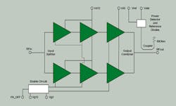
Figure 1 depicts the block diagram of the PA integrated circuit (IC). It consists of two equal three-stage PAs that are joined at the input by an in-phase power splitter and at the output by an in-phase power combiner. Located after the power combiner is a compact directional coupler used for power-detection purposes. The coupled signal is rectified by a forward-biased detector diode, which has a temperature-compensated characteristic thanks to an identical and equally forward-biased reference diode. The temperature-compensated detector output is given by “Vref – Vdet,” which can be readily monitored by an analog-to-digital converter (ADC).
1. The integrated power-amplifier IC features two three-stage PAs.
Also included is a fast-switching enable circuit, which is controlled by the logic signal “PA_OFF.” This can be used to rapidly power up and power down the PA such that it draws just 0.1 mA of current when not in use, thus maximizing overall system efficiency. In power-down mode, “PA_OFF” is set to +2.5 V; in normal operation, it’s set to 0 V.
During operation, the PA is typically backed-off from compression to preserve modulation fidelity of the transmitted signal. With this in mind, the design approach adopted involved optimizing the PA’s performance when operating at 7-dB back-off from 1-dB compression (P1dB). A deep Class AB bias scheme was utilized so that the power-added efficiency (PAE) could be optimized at this operating point.
The design commenced by selecting the optimum transistor size for the output stage, followed by load-pull simulation trials to assess the optimum impedances for best linearity and PAE at back-off at different quiescent bias conditions. The tradeoff in gain, linearity, and PAE was then evaluated and the optimum bias condition determined.
Optimum transistor sizes for the driver and pre-driver stages were selected as the design of the complete three-stage PA progressed. Again, careful tradeoffs were considered. Larger transistor sizes improve the overall linearity but reduce the PAE. With the size and bias of all transistors selected, the detailed design of the matching and biasing circuitry could proceed.
The layout was considered from an early stage of the design process to ensure that a practical implementation was possible without incurring unacceptable parasitics. A common gate bias line was used for stages one and two (applied at pin PA_Vg12). A separate bias line was used for stage three (PA_Vg3). This allowed for the possibility of separately optimizing the two voltages for potential linearity or PAE improvements to the PA. The drain supplies were similarly applied through two separate pins. However, these were connected on the printed circuit board (PCB) used to evaluate the packaged parts. The +4-V drain supply is applied at “PA_Vd12” and “PA_Vd3.”
To ensure good RF performance, careful electromagnetic (EM) simulation was essential. A step-by-step approach was adopted, adding each part of the circuit to the EM simulation one at a time, with the rest of the circuit still being simulated using process-design-kit (PDK) models. As the IC was destined for packaging in an overmolded plastic package, the EM simulation also needed to account for the presence of the molding compound atop the IC.
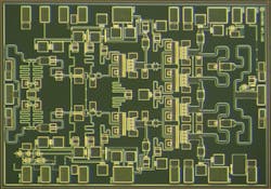
Figure 2 is a photograph of the PA die. The engineering die size measures just 2.85 × 1.99 mm, but this can be reduced to 2.85 × 1.85 mm for mass production. Its pad/pin positions are similar to those shown in the block diagram (Fig. 1, again), although it incorporates a number of GND pads to make it fully RF-on-wafer (RFOW) testable. RFOW test also requires that the drain voltages are applied at each side. When assembled in a package, however, the drain bias only needs to be applied on one side.
2. The size of the PA die is a mere 2.85 × 1.99 mm.
The IC was designed to be packaged in a low-cost plastic overmolded 4- × 4-mm QFN. In addition, to account for the effects of the molding compound, the RF transition from IC to PCB needed to be carefully optimized. A custom leadframe was designed to facilitate this operation, and the RF ports of the package are all implemented as ground-signal-ground interfaces.
Measured and Simulated Performance
Prior to packaging, several of the die were tested RFOW, which confirmed that the first pass design had been successful (the RFOW results are not presented here). All measurements were made on a packaged assembled IC mounted on a representative evaluation PCB.
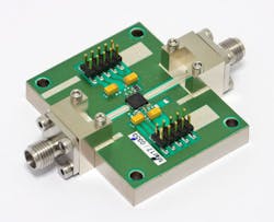
The evaluation PCB was designed using a low-cost laminate PCB material suitable for volume mass production. Samples of the packaged PAs were assembled onto the evaluation PCBs. All of the measured performance is calibrated to the package pins on the evaluation PCB and includes the effects of the IC-to-PCB transition. A thru-reflect-line (TRL) calibration tile was designed to allow for calibration of the measured performance to the reference planes of the package. Figure 3 shows a photograph of one of the evaluation PCBs.
3. Here, the PA is housed on an evaluation board.
All of the measured results presented correspond to the packaged PA monolithic microwave integrated circuit (MMIC) mounted on the PCB. The measurements are referenced to the RF pads of the package. Throughout the evaluation, a commercially available multichannel digital-to-analog converter (DAC) and ADC IC was used to control and monitor the PA. Conveniently, the PA does not require any negative voltages, since it was designed on an enhancement-mode process.
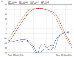
Figure 4 compares the measured-to-simulated S-parameters of a typical PA. The solid traces represent the measured data, while the dashed traces depict simulated results. The PA is biased to around 180 mA total quiescent current from +4 V. Small-signal gain (S21) is above 20 dB from 27 to 29 GHz. The input return loss (S11) is better than 16 dB across the band. The output is matched for best PAE at back-off rather than best S22, but the measured S22 (not shown) is 8 dB or better across the band.
4. Measured and simulated PA S-parameters are plotted.
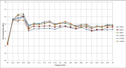
To reflect the wide channel bandwidths anticipated in 5G systems, the output-referred third-order intercept point (OIP3) of the PA was evaluated with a tone spacing of 100 MHz. The measured OIP3 of a typical PA is plotted in Figure 5, with the wanted output tone powers ranging from +7 to +17 dBm per tone. One can see that the OIP3 is around +32.5 dBm across the 5G band and shows very little variation with tone power over a 10-dB dynamic range.
5. Shown is measured OIP3 versus frequency for different input tone levels.
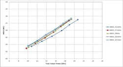
The data was rearranged to plot IMD3 versus total output power (Fig. 6). This indicates that at an operating point of around +18 dBm, the corresponding IMD3 is −35 dBc. This key target performance parameter—among others—was successfully met.
6. Measured IMD3 versus output power is given at five different frequencies.
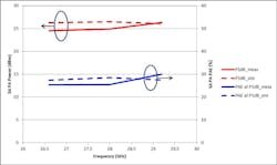
To provide a figure of merit for comparative purposes, the output-referred P1dB and PAE were also measured, although 5G systems will require linear amplification to preserve modulation fidelity. The measured performance is plotted in Figure 7 using solid traces, revealing a P1dB around +25 dBm. The corresponding PAE is around 25.5%, rising to 30% at the top of the band. Figure 7 also shows the simulated P1dB and corresponding PAE (dashed traces), which are in good agreement with the measured data.
7. In terms of measured and simulated P1dB and PAE versus frequency, a measured P1dB of about +25 dBm was achieved.
As mentioned above, the PA is designed for optimum performance (OIP3 and PAE) when operated at around 7-dB back-off from P1dB, or more specifically, with the third-order intermodulation products (IMD3) at a level below −35 dBc relative to the wanted products during a two-tone test with 100-MHz tone spacing. This operating point is close to that envisaged in the 5G system for which the PA was designed.
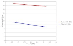
Figure 8 shows a plot of the measured-to-simulated PAE and total RF output power when operating at an IMD3 point of −35 dBc. The measured PAE is 8%, which is a good result and largely due to the PA being designed to operate in deep Class AB. The total RF output power is around +18 dBm, which equates to an OIP3 level of +32.5 dBm.
8. This is the measured power and PAE operating at about 7-dB back-off.
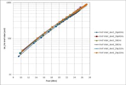
A dc voltage that enables monitoring of the RF output power is provided by the on-chip transmit (Tx) power-detector characteristic. In Figure 9, the temperature-compensated detector output “Vref-Vdet” is plotted in mV on a logarithmic scale against output power in dBm for two devices each measured at three frequencies over a 17-dB dynamic range. On this scale, the characteristics are very similar—and linear—which simplifies power monitoring.
9. On-chip power-detector outputs of two PAs were measured.
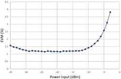
The PA’s performance was also evaluated using a real wideband 5G signal. The selected test signal was an OFDM waveform of 400-MHz bandwidth with 120-kHz subcarrier spacing using 64-QAM modulation. The waveform has a high peak-to-average ratio of 11.71 dB. The error vector magnitude (EVM) against input power at 28 GHz when the PA is transmitting this signal (Fig. 10) indicates that the PA has a high degree of linearity. At an operating point of +18 dBm average output power, the input power is −3 dBm and the EVM is less than 4%. The corresponding PAE at this operating point is 8%.
10. This is the EVM versus PA input power at 28 GHz. The conditions included OFDM waveform, 400-MHz bandwidth, and 64 QAM.
Summary and Conclusions
The PA MMIC described here will potentially play a vital role in 28-GHz 5G systems. The part, which has been shown to address all of the requirements for integration into mmWave phased-array or beam-switched terminals, offers excellent linearity and efficiency. The key performance specifications were met, ensuring that the part is highly suitable for mmWave 5G applications.
The IC also includes useful features, such as a Tx power detector and an enable circuit. Realized on a state-of-the-art 0.15-µm enhancement-mode GaAs P-HEMT process, the part is extremely easy to control and monitor using widely available multichannel ADC and DAC ICs. In addition, the part is conveniently housed in a compact and low-cost 4- × 4-mm plastic overmolded QFN SMT package. At an operating point of +18 dBm, the PA has a PAE of 8% and achieves an EVM of less than 4% for a 400-MHz-wide 5G waveform with a high peak to average ratio of 11.7 dB.

