This file type includes high resolution graphics and schematics when applicable.
Metamaterials offer great promise in the design of high-frequency components, such as antennas. If properly applied, these engineered materials can enable, for example, enhanced antenna directivity for compact microstrip designs.
To demonstrate, Z-type and quasi-triangular metamaterials were applied to conventional microstrip circuitry to produce an antenna substrate with improved electromagnetic (EM) radiation characteristics. These metamaterials effectively minimize backward-wave radiation while increasing forward antenna radiation, resulting in a directivity factor increase of 92.6% and gain increase of 3.03 dB for an experimental 6-GHz microstrip antenna.
Metamaterials have been considered part of certain design efforts since 1968, as a potential means of improving antenna performance.1 Because of its small size and ease of integration into many different high-frequency circuits, microstrip antennas have been quite popular for use at microwave frequencies. Unfortunately, the low directivity and high loss of microstrip antennas has limited their use in some applications.
To increase the usefulness of microstrip antennas, research was performed to better understand how metamaterials might be used to increase antenna gain and directivity. Traditional methods of antenna optimization have rarely improved upon the limits of physical size, bandwidth, and gain, so it was thought that using metamaterials as part of the construction might improve microstrip antenna performance.2-6
Some research groups have made use of convergence effects to improve antenna performance with metamaterials,7-13 while other groups have employed metamaterials and the backward-wave characteristics of different antenna designs to achieve smaller physical designs.14-16 Some workers have proposed the use of absorbing materials to reduce antenna loss.17 Some studies have used metamaterials both as an antenna substrate material and as an overlay material for the antenna, but those studies have lacked details on covering materials for those antenna designs.
The current report presents a microwave frequency microstrip antenna built on a metamaterial medium. Metamaterials are used both for the substrate and the cover layer. Computer-aided-engineering (CAE) simulation was performed to explore the influence of the metamaterials, including the cover layer, on antenna performance. The analysis reveals that the use of metamaterials in the substrate and covering layer significantly improves the gain, directivity, and radiation efficiency of the antenna compared with a microstrip antenna fabricated on conventional circuit materials.
This file type includes high resolution graphics and schematics when applicable.
The Optical Advantage
This file type includes high resolution graphics and schematics when applicable.
By using the optical properties of metamaterials, it is possible to control the permittivity and permeability of the materials to a degree. Using metamaterials as an antenna cover layer improves antenna directivity based mainly on the near-zero refractive characteristic of the materials.
According to Snell’s law, which describes the angles of incidence for different waves and their refraction through different materials, EM waves build to propagate in a particular direction. Assuming that an EM wave from a metamaterial medium is incident to an air medium, and the EM wave vector is in the x-z vector, the wave vector can be described as
For transverse electromagnetic (TE) wave propagation, the polarization direction of the electric field is along the y-axis direction, where ky = 0, and
The two components of the refractive index are
and
nz =
(μrxεry)0.5
When
|μrz| << 1,
nz ≈ 0, nx ≠ 0,
then
kz ≈ 0, kx >> 0.
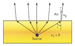
Since the propagation of EM waves must comply with the phase-matching conditions and the z-axis of the antenna structure is along the surface between the metamaterials and the air medium, the EM wave radiation builds near the normal vector of the interface between the air and the EM propagating medium (Fig. 1).
The use of metamaterials for an antenna substrate can minimize problems caused by strong surface waves. When an EM wave is incident to the surface of a lossy medium or nonideal conductor, a surface wave is generated. It usually appears as part of the TM wave on a capacitive surface, or a TM wave on an inductive surface. It is commonly used as part of the nonzero thickness of the dielectric substrate.
When the relative permittivity of the substrate is εr > 1 (higher than air), at least one transverse-magnetic (TM) propagating mode has a cutoff frequency of zero, which is known as the TM0 mode. In practice, a substrate’s length is limited. A substrate edge antenna will produce large amounts of radiation sidelobes with a zero corner, while the substrate back edge will produce EM radiation. Consequently, much energy is wasted in the back hemisphere, which impacts on antenna performance.
Metamaterials used as antenna substrates are optimized according to their negative permittivity characteristics. They are optimized to suppress the undesired radiation generated by any surface waves. Any metamaterial design can be analyzed by the equivalent-circuit method, where the design of a circuit with metamaterials is essentially the same as an equivalent circuit with impedance of
From this impedance formula, it can be seen that the impedance approaches infinity when metamaterial unit reaches the resonant frequency, thus prohibiting the radiation of a surface wave.
This file type includes high resolution graphics and schematics when applicable.
Designing the Antenna
This file type includes high resolution graphics and schematics when applicable.
Parallel to the y-axis, two planes were set for perfect magnetic conductor (PMC), two planes parallel to the x-axis is set for perfect electric conductor (PEC). Metal structures on both sides of the substrate in the magnetic field induce antiparallel currents to achieve magnetic resonance. The structure of the metal rod will produce an electric-field-induced resonance. By optimizing and adjusting the dimensional parameters, a desired resonant frequency can be achieved with these metamaterial antenna structures.
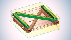
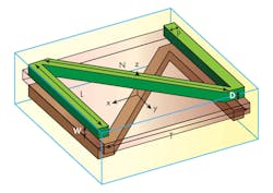
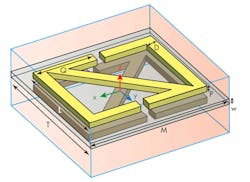
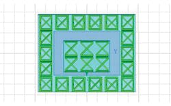
The Z-type structure was printed on both sides of double-sided FR-4 printed-circuit-board (PCB) material. The FR-4 was 1.6-mm thick with relative dielectric constant, εr, of 4.4. The geometric parameters of the Z-type structure were T = 7.5 mm; W = 1.6 mm; L = 6 mm; N = (2)0.5L; P = 0.2 mm; and D = 0.3 mm. The quasi-triangular structure was printed on both sides of a 1.6-mm-thick FR-4 board with εr of 4.4. The geometric parameters for this structure were T = 8 mm; W = 1.6 mm; M = 8 mm; P = 0.3 mm; L = 6.5 mm; D = 0.5 mm; and Q = 2.8 mm.
The cladding layer for the Z-type unit was based on the principle of the zero refractive property of metamaterials; the antenna substrate production of the quasi-triangular metamaterial unit is due to the use of the transmission bandgap effect. An ASUS computer running the High Frequency Structure Simulator (HFSS) electromagnetic (EM) simulation software from ANSYS was used for the simulation of these structures, based on the finite-element method of simulation. The border of the simulation calculations was 8 × 8 × 8 mm3.
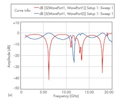
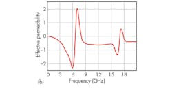
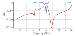
These simulations yielded S-parameters for the Z-type structure [Fig. 4(a)]. In addition, the permittivity of the Z-type unit was calculated [Fig. 4(b)] by means of the Matlab software from Mathworks and the use of the NRW algorithm.17 The results show that a zero refractive index can be achieved at 6 GHz. The S-parameters for the Z-type unit (Fig. 5) indicate that the 6-GHz band gap that appeared in these results can be used to improve the performance of that antenna structure.
This file type includes high resolution graphics and schematics when applicable.
Working in Reverse
This file type includes high resolution graphics and schematics when applicable.
A form of reverse thinking helped to design the metamaterial antenna structural units. First, the specific requirements of an application are determined, then the structure is designed, and finally the structure’s parameters are adjusted to meet the requirements of the application. HFSS was used to design and simulate the performance of a microstrip antenna with center frequency of 6 GHz. The antenna, which was based on FR-4 PCB material with relative dielectric constant, εr, of 4.4 at 10 GHz in the z-axis (thickness) of the material.
The material was 1.6-mm thick and a 50-Ω feeder was designed as part of the antenna. The width of the antenna’s radiation patch was w = 16 m with length, L, of 10.8 mm. The feed point position for the antenna was at L1 = 2.7 mm. The width and length of the dielectric substrate were W0 = 47 mm and L0 = 37.5 mm, respectively.
In keeping with the 6-GHz center frequency, the cover layer of the Z-type structure is disposed above the microstrip antenna by means of a double-layer structure. A distance of 3 mm is between the two cover layers. The lower distance between the cover and the antenna is 33 mm.
Adjusted quasi-triangular metamaterial units were printed on a substrate, with the metamaterial unit printed around the radiation patch. To ensure use of the material’s zero refractive properties and bandgap characteristics, the microstrip antenna’s center frequency should be the same as that of that of the two metamaterial units (Fig. 6).
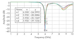
Simulations provided return-loss values for four types of experimental antennas: one with the metamaterial layer and substrate as a covering, the metamaterial unit with the substrate alone, the unit with separate loading cover layer, and the original antenna (Fig. 7). The maximum return loss for all four devices occurred at the center of each microstrip antenna, with the peak value of loss at different values for the four approaches. The results show that the impedance matching performance of the antenna has been optimized.
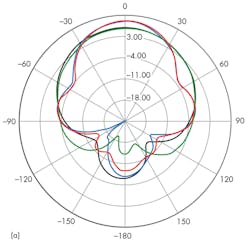
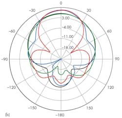
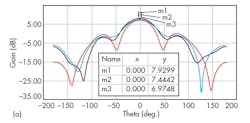
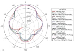
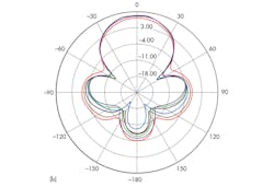
Gain patterns were also obtained at the center frequency for these four antenna configurations (Fig. 8). Compared to an standard microstrip antenna, using metamaterials to cover both the layer and the substrate, the E- and H-plane half-power (-3-dB) beamwidths of the antenna were reduced by 47.5 and 37.1 deg., respectively. If the metamaterials are only used as overlay for the antenna, the half-power beamwidths are reduced by 36.7 and 28.3 deg., respectively.
If the metamaterials are only used for the antenna substrate, the radiation will be 9.7 and 7.57 deg., respectively. As shown in this report, with metamaterials, the antenna substrate wave radiation was reduced by nearly one-half that of a conventional microstrip antenna.
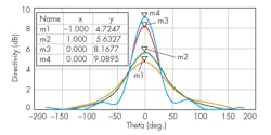
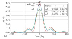
Directivity coefficients were also plotted (Fig. 9). When using metamaterials, both as the dielectric layer and the substrate loading covering layer alone, and making substrate alone—as well as dividing the directivity of the original antenna as 9.09, 8.17, and 5.63 dB—it can be seen that the directivity coefficients are increased by 4.37, 3.45, and 0.91, respectively. These are relative increases of 92.6, 73.09, and 19.28 deg., respectively.
The geometry of these metamaterial antenna units must be optimized to match the center frequency of a microstrip antenna for optimum results. Also, the metamaterial cover layer must be loaded over the top of the antenna, at an optimum distance to the antenna along with optimum number of cover layers and optimum distance between layers.
The back radiation of an antenna loaded with cover increases with the increase in spacing between the cover layer and the antenna. This is due to the restriction of EM radiation and the fact that the EM energy forms a loop between the antenna substrate and the cover layer. The back radiation of the antenna substrate to the EM wave increases.
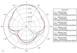
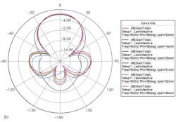
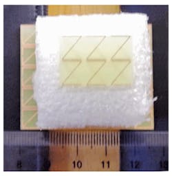
In the experimental covered design, the distance between the middle and the experimental layer was 3 mm [Fig. 11(a)]. The simulations were limited to three covering layers due to the capabilities of the computers used in the simulation. Even with only three layers, the trends show increased control of the EM wave propagation orientation for the antenna. The gain tends to decrease, however, with the addition of more covering layers.
The antenna gain was evaluated for two covering layers, with gain varying with the distance between the covering layers (Fig. 12). With the increasing distance between the two cover layers, the antenna gain and directivity coefficients first increase and then decrease. There are two reasons for this phenomenon. On one hand, reflection of the EM waves is large with large distance between the covering layers. On the other hand, if the distance is too small, resonance occurs between the different units. As a result, the resonant frequency shifts so that the center frequency of the metamaterial structure and the antenna are not properly matched.
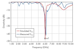
Variations occur in reflection coefficient for different metamaterial conditions (Fig. 13). The antenna shows a -42-dB level at 6.1 GHz. These simulations turned out to be fairly close to measured results for an antenna and structure that was finally fabricated.
The Z-type and quasi-triangular metamaterial antenna units were loaded to ordinary coaxial-feed microstrip lines. The antenna covering layers were formed from zero-refractive materials to optimize antenna directivity. The bandgap properties of the material suppressed surface waves and reduced antenna backward wave loss.
Without changing the original microstrip patch antenna size, the use of metamaterials made it possible to nearly double antenna directivity. The E- and H-field half-power (-3-dB) beamwidth was contracted by 47.5 and 37.1 deg., and the forward radiation increased. By suppressing backward-wave radiation, antenna gain increased by 3.03 dB. By optimizing the coating layer, it is possible to further improve antenna performance compared to conventional microstrip antennas without the use of metamaterials.
Acknowledgements
This work was supported by the National Natural Science Foundation of China (Grant No. 61072034), the National Nature Science Foundation of China (Grant No. Q1302316), the National Natural Science Foundation of China (Grant No. 61265006), and the Basic Research Project of Engineering University of CAPF (Grant No. WJY201404).
Xiangjin Quan, Professor
Shiquan Zhang, Associate
Hui Li, Associate
Engineering University of CAPF, Xian 710086, People's Republic of China
This file type includes high resolution graphics and schematics when applicable.
References
This file type includes high resolution graphics and schematics when applicable.
1. V.G. Veselago, “The electrodynamics of substances with simultaneously negative values of ε and μ,” Journal of Soviet Physics Uspecki, Vol. 10, No. 4, 1968, pp. 509-514.
2. R. Yang, Y. Xie, P. Wang, et al., “Characteristics of millimeter wave microstrip antenna with left-handed materials substrates,” Journal of Applied Physics Letters, Vol. 89, 2006, pp. 64-108 (1-3).
3. H. Mosallaei and K. Sarabandi, “Antenna miniaturization and bandwidth enhancement using a reactive impedance substrate,” IEEE Journal of Transactions on Antennas and Propagation, Vol. 52, No. 9, 2004, pp. 2403-2414.
4. Y.H. Liu and X.P. Zhao, “Investigation of anisotropic negative permeability medium cover for patch antenna,” IET Journal of Microwaves, Antennas, and Propagation, Vol. 7, No. 2, 2008, pp. 737-744.
5. Y.H. Liu and X.P. Zhao, “Enhanced patch antenna performances using dendritic structure metamaterials,” Journal of Microwave and Optical Technology Letters, Vol. 51, No. 7, 2009, pp. 1732-1738.
6. H.F. Tang and X.P. Zhao, “Center-fed circular epsilon-negative zeroth-order resonator antenna,” Journal of Microwave and Optical Technology Letters, Vol. 51, No. 10, 2009, pp. 2423-2428.
7. T.C. Han, M.K.A. Rahim, T. Masri, et al., “Left-handed metamaterial design for microstrip antenna application,” Proceedings of the Asia-Pacific Microwave Conference. Bangkok, Thailand, December, 11-14, 2007, pp. 1-4.
8. G. Wang, J.R. Fang, and X.T. Dong, “On the use of LHM lens for near-field target detection and imaging,” 7th International Symposium on Antennas, Propagation, and EM Theory, Guilin, October 26-29, 2006, pp. 1-4.
9. A.M.G. Alu, A. Silveirinha, A. Salandrino, and N. Engheta, “Epsilon-near-zero metamaterials and electromagnetic sources: Tailoring the radiation phase pattern,” Physical Review B, Vol. 75, 2007, pp. 155-410.
10. Zhang Fushun, Shang Yuanbo, Zhang Tao, et al., “A circular polarization microstrip array with high-gain and low-side lobe,” Chinese Journal of Radio Science, Vol. 23, No. 3, 2008, pp. 572-575. (in Chinese).
11. R. Yang, Y. Xie, P. Wang, et al., “Characteristics of millimeter wave microstrip antenna with left-hand materials substrates,” Applied Physics Letters, Vol. 89, Nos. 1-3, pp. 64-108, 2006.
12. J.B. Pendry, D. Schurig, and D.R. Smith, “Controlling Electromagnetic Fields,” Science, Vol. 312, 2006, p. 1780.
13. Q. Wu, P. Pan, F.Y. Meng, L.-W. Li, and J. Wu, “A novel flat lens horn antenna designed based on zero refraction principle of metameterials,” Applied Phys. A, Vol. 87, 2007, pp. 151-156.
14. S. Hrabar, D. Bonefacic, and D. Muha, “Application of wire-based metamaterials for antenna miniaturization,” 3rd European Conference on Antennas and Propagation, Berlin, Germany, March 23-27, 2009, pp. 620-623.
15. P. Mookiah and K. R. Dandekar, “Metamaterial-substrate antenna array for MIMO communication system,” IEEE Transactions on Antennas & Propagation, Vol 57, No. 10, 2009, pp. 3283-3292.
16. H. Mosallaei and K. Sarabandi, “Antenna miniaturization and bandwidth enhancement using a reactive impedance substrate,” IEEE Transactions on Antennas and Propagation, Vol. 52, No. 9, 2004, pp. 2403-2414.
17. W. Zhu, X. Zhao, and B. Gong, “Left-handed metamaterials based on a leaf-shaped configuration,” Journal of Applied Physics, 2011, 109(9): 093504-093504-5.
This file type includes high resolution graphics and schematics when applicable.
