Quadrupler Cuts Losses At W-Band
This file type includes high resolution graphics and schematics when applicable.
Schotty diode quadruplers provide practical means of generating signals at higher frequencies, especially when they can perform such functions with minimal conversion loss (CL). Lower loss generally means higher power levels at the output of the quadrupler. Fortunately, with the aid of a commercial computer-aided-engineering (CAE) software program, it has been possible to design a Schottky diode multiplier with low CL for applications requiring signals from 80 to 100 GHz. This monolithic frequency multiplier was fabricated with a 0.1-μm GaAs pseudomorphic-high-electron-mobility-transistor (pHEMT) process, providing as much as +2 dBm output power across its 20-GHz output bandwidth.
Due to their nonlinear characteristics, Schottky diodes are often the key elements in passive frequency multipliers. They are capable of producing stable, low-noise multiplied output signals when combined with an appropriate oscillator.1 Unfortunately, as the frequency increases, the dielectric circuit losses and roughness of the conductor surface can result in increases in the CL of a Schottky diode multiplier. As a result, one of the design goals when working with these components involves minimizing the CL.
A number of researchers have explored different approaches to passive multiplier designs,2-4 with the importance of impedance matching for the source and load impedances of the Schottky diodes detailed in ref. 2 (although an impedance-matching method or solution was not provided). A W-band frequency doubler was presented in ref. 3, with a quarter-wavelength short stub (at the fundamental frequency) used to provide a short circuit for the second-harmonic frequency at the input of the diode, and a quarter-wavelength open stub (at the fundamental frequency) used to short the fundamental frequency at the output of the diode. This study did not present the effects of these stubs on CL performance, however. A similar design approach was presented in ref. 4.
Work in ref. 5 detailed a method for optimizing the input and output impedances to a high-gain active frequency multiplier with reflector networks. A similar approach was used in ref. 6 to optimize a frequency tripler. A W-band active frequency doubler was designed and fabricated with a 0.15-μm InGaAs/InAlAs/GaAs mHEMT process in ref. 7. These reports offered several different approaches for designing high-frequency multipliers, but with little description of CL optimization methods for the passive balanced multipliers. The present report examines the importance of impedance matching for the input and output multiplier ports, using input and output reflector networks to not only impedance match to the impedances of the diodes, but also reduce the CL of the balanced multiplier.
One method of reducing the CL of a diode multiplier is to focus on the Schottky diode and its supporting circuitry. This can be done by examining the construction of a Schottky diode quadrupler, the design of the component’s balun, optimization of the input power network and the input/output reflector networks; optimizing the full quadrupler; and fabricating and testing the quadupler to check how the modeled results compare with actual performance. Figure 1 offers a block diagram of a generic balanced multiplier, with an antiparallel diode-pair structure used with a balanced-mixer configuration.8 In this configuration, only even-harmonic frequencies are available at the output, with inherent rejection fundamental-frequency and odd-harmonic signals at the output.
As Eq. 1 shows, the nonlinear Schottky diode current-voltage (I-V) curves are closely related to the input signal amplitude. The input power can be optimized to obtain minimum CL from the multiplier by analysis of Eq. 1:
I = I0[exp(VA/VT) – 1] (1)
where:
I0= the reverse saturation current;
VA = the diode external voltage; and
VT = the thermopower voltage;
Equations 2 and 3 show that the signals reflected by different reflector networks have different phase characteristics. Short-circuit (SC) transmission-line voltage is a sinusoidal function, but open-circuit (OC) transmission-line voltage is a cosine function. Changing the type of transmission line can optimize the performance of the multiplier. The voltage of an SC transmission line can be found by studying Eq. 2, while the voltage of an OC transmission line can be calculated by Eq. 3:
V(d) = 2jV+sin(βd) (2)
V(d) = 2V+cos(βd) (3)
where:
V+ = the voltage amplitude of the electromagnetic (EM) wave propagating along the positive direction;
β = the phase constant of the transmission line; and
d = the length of the transmission line.
As a result, it is necessary to optimize the input-power network and the input/output reflection networks to minimize the CL of a high-frequency multiplier design.
This file type includes high resolution graphics and schematics when applicable.
Marchand Balun Design
This file type includes high resolution graphics and schematics when applicable.
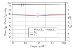
A Marchand balun is often part of the design of balanced multipliers, mixers, and amplifiers. The balaun can be designed in a number of different ways, with multiple planar balun structures proposed in ref. 9. The balaun shown in Fig. 2 offers a similar design. From a study of Fig. 3, it is possible to learn that (a) the phase difference (P2 minus P3) is 185 to 190 deg. between 80 to 100 GHz, and (b) the insertion loss (from P2 to P1 and from P3 to P1) is less than 3.6 dB from 80 to 100 GHz.
The input-power network and the input/output reflector networks can be optimized with the assistance of computer analysis using the Advanced Design System (ADS) software from Agilent Technologies and load-pull technology for analysis. It is well known that the output port of a balanced frequency multiplier will only contain even-harmonic signals and, according to the nonlinear characteristics of the multiplier, the impact of CL is weak on the higher multiplied harmonic signals. Consequently, analysis at the input port of the multiplier can focus on the input power, the fundamental-frequency signals, and the second- and fourth-harmonic signal impedance at the multiplier’s input port.
In addition, the second-, fourth-, and sixth-harmonic impedances at the output port of the multiplier should also be studied. The input and output reflector networks for the multiplier include SCs, OCs, and matching circuits (MCs).
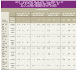
Table 1 provides data for analysis of CL performance for different networks, making it possible to draw a number of conclusions. For one thing, a change of CL impacted by the second- or fourth-harmonic reflector networks at the input port is about 0.1 dB, and this can be ignored. The appropriate input fundamental-frequency power reduces the VCL by about 1 dB, so the level of the fundamental input power should be a concern in the design of a frequency multiplier. When the second-harmonic reflector network is an open circuit at the output port, the CL is reduced by about 1 dB, which is an important consideration.
Also, when the six-harmonic reflector network is an open circuit at the output port, the CL is reduced by about 0.2 to 0.4 dB—not a small amount of loss. According to these data, it is possible to optimize a Schottky diode multiplier for certain operating conditions. The specific structure is shown in Fig. 4.
This file type includes high resolution graphics and schematics when applicable.
Quadrupler Layout
This file type includes high resolution graphics and schematics when applicable.
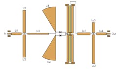
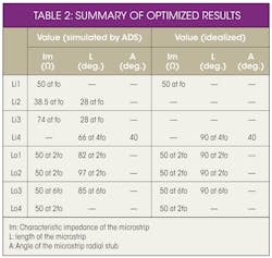
As the studies show, a number of conclusions can be drawn. For one, the input reflector networks have been used to both impedance-match the fundamental-frequency signals and short-circuit the second- and fourth-harmonic signals. The output reflector networks are used to both impedance-match the fourth-harmonic signals and open-circuit the second- and sixth-harmonic signals. As shown in Fig. 5 and Table 2, the quadrupler’s specific layout can be obtained by analysis of these matching requirements.
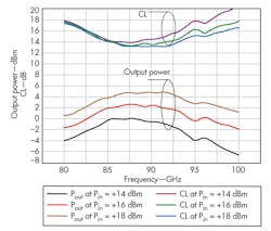
By using commercial analysis software such as ADS, it is also possible to determine the output power (based on an input-power level) and the CL curves for a frequency-multiplier design. From such computer simulation curves, the maximum output power point and minimum CL point for the quadrupler is found to be near 87 GHz when the input power is around +20 dBm. The minimum CL is around 13 dB and the output power is around +7 dBm. This quadrupler design was realized with a 0.1-μm-gate-length GaAs pHEMT process, with the quadruplier chip, which measures 0.8× 1.6 mm, shown in Fig. 6.
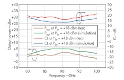
The device was testing in a Class 10,000 cleanroom, measured on wafer using a model M150 probe station from Cascade Microtech, a model ACP110-S ground-signal-ground (GSG) W-band probe from Cascade Microtech, and a model W8486A W-band power probe from Agilent Technologies. Simulated and measured results are compared in Fig. 7, showing that the output frequency characteristics between modeled and measured results are somewhat offset. This is most likely because the Schottky diode model may not be totally accurate, since the quadrupler works at W-band frequencies. In addition, because of the fabrication precision and dielectric losses, differences may exist between the simulated results and the actual measurements.
Still, it was possible to simulate the performance of a Schottky diode multiplier from 80 to 100 GHz with results that were fairly close to the measurements of an actual fabricated quadrupler for that same frequency range. The analysis showed that it is possible to reduce the multiplier’s CL, provided that the input-power network and the input/output reflector networks are fully optimized. The monolithic quadrupler that was finally fabricated can produce output levels of about -3 to +2 dBm across the target frequency range of 80 to 100 GHz.
Yong Fang, Doctor
Hai Zhang, Doctor
National Key Laboratory of Science and Technology on Vacuum Electronics, School of Physical Electronics, University of Electronic Science and Technology of China, Chengdu (610054), People’s Republic of China; e-mail: [email protected]
Baoqing Zeng, Professor
National Key Laboratory of Science and Technology on Vacuum Electronics, School of Physical Electronics, University of Electronic Science and Technology of China, Chengdu (610054), People’s Republic of China
Department of Electronic Engineering, University of Electronic Science and Technology of China Zhongshan Institute, Zhongshan (528402), People’s Republic of China
Tiguo Gan, Professor
10th Institute of China Electronic Technology Group Corporation, Chengdu (610036), People’s Republic of China
Ye Yuan, Doctor
School of Electronic Engineering, University of Electronic Science and Technology of China, Chengdu (610054), People’s Republic of China; e-mail: [email protected]
This file type includes high resolution graphics and schematics when applicable.
References
This file type includes high resolution graphics and schematics when applicable.
1. Y. Campos-Roca, L. Verweyen, M. Fernández-Barciela, E. Sánchez, M. C. Currás-Francos, W. Bronner, A. Hälsmann, and M. Schlechtweg, “An optimized 25.5–76.5 GHz pHEMT-based coplanar frequency tripler,” IEEE Microwave & Guided Wave Letters, Vol. 10, No. 6, June 2000, pp. 242–244.
2. S.A. Maas and Y. Ryu, “A broadband, planar, monolithic resistive frequency doubler,” IEEE Microwave and Millimeter-Wave Monolithic Circuits Symposium, 1994, pp.175-178.
3. G. Hegazi, A. Ezzeddine, F. Phelleps, P. McNally, K. Pande, P. Rice, and P. Pages, “W-band monolithic frequency doubler using vertical GaAs varactor diode with n+ buried layer,” Electronics Letters, Vol. 27, No. 3, January 1991, pp. 213-214.
4. S. Chen, T.C. Ho, K. Pande, and P.D. Rice , “ Rigorous analysis and design of a high-performance 94 GHz MMIC doubler,” IEEE Transactions on Microwave Theory & Techniques, Vol. 41, No. 12, December 1993, pp. 2317-2322.
5. D.G. Thomas, Jr. and G.R. Branner, “Single-ended HEMT multiplier design using reflector networks,” IEEE Transactions on Microwave Theory & Techniques, Vol. 49, No. 5, May 2001, pp. 990-994.
6. J.E. Johnson, G.R. Branner, and J.P. Mima, “Design and optimization of large conversion gain active microwave frequency triplers,” IEEE Microwave & Wireless Components Letters, Vol. 15, No. 7, July 2005, pp. 457-459.
7. Dong Min Kang, Ju Yeon Hong, Jae Yeob Shim, Jin-Hee Lee,Hyung-Sup Yoon, and Kyung Ho Lee, “A 77 GHz mHEMT MMIC Chip Set for Automotive Radar Systems,” ETRI Journal, Vol. 27, No. 2, April 2005, pp.133-139.
8. Bong-Su Kim, Woo-Jin Byun, Min-Soo Kang, and Kwang Seon Kim, “E-Band Wideband MMIC Receiver Using 0.1 μm GaAs pHEMT Process,” ETRI Journal, Vol. 34, No. 4, August 2012, pp.485-491.
9. W.M. Fathelbab, and M.B. Steer, “New classes of miniaturized planar marchand baluns,” IEEE Transactions on Microwave Theory & Techniques, Vol. 53, No. 4, April 2005, pp. 1211-1220.
This file type includes high resolution graphics and schematics when applicable.
