Cost-Effective Models Simulate SMT Components
This file type includes high resolution graphics and schematics when applicable.
Accurate models of surface-mount-technology (SMT) components are often required when using modern high-frequency computer-aided-engineering (CAE) circuit simulators. This is becoming more commonplace as the frequency range and use of available high-frequency SMT components increases. Accurate models mean fewer design iterations, less troubleshooting, and shorter time to market for a design. Fortunately, such models can be derived from S-parameter measurements—but those S-parameter measurements must be sufficiently reliable to ensure model accuracy.
Obtaining reliable S-parameters of an SMT component is not a straightforward process because the component needs to be mounted on a test jig. Therefore, the combined response of the SMT component and the test jig is measured by the measurement system and the electrical contributions of the test jig must subsequently be removed. The process becomes more difficult as the frequency of the SMT component rises.
There are several ways of measuring the S-parameters of an SMT component using a vector network analyzer (VNA).1,2 These include port extension, de-embedding, and calibration on a printed circuit board (PCB). Other approaches, such as thru-reflect-line (TRL) techniques, can work well but are difficult to use with wide (decade or greater) bandwidths, particularly when extended to lower frequencies.
Port extension is the simplest approach. With this technique, coaxial cables are connected to the VNA and a calibration is performed by attaching coaxial calibration standards to the ends of the cables. The measurement reference planes are then established at the ends of the cables. Then, the test jig containing the SMT component is connected to the cables and the measurement reference planes are extended (using the VNA’s electrical delay capability) to the mounting pads of the SMT device.
The disadvantage of this approach is that effects due to impedance mismatches (for example, from coaxial-to-microstrip connectors on the test jig) are not removed from the measurements. In addition, losses associated with the microstrip lines on the test jig that connects to the SMT component are difficult to remove from the measurements.
De-embedding methods require that each half of the test jig is characterized separately. This is usually achieved by using a VNA to measure each half of the test jig as a twoâport network. The SMT component is then inserted between the two halves of the test jig and the combination of test jig and SMT component is measured using the VNA. The test jig information (i.e., the S-parameters of each half of the test jig) is then used to mathematically remove (de-embed) the effects of the test jig from the overall measurement of the combined test jig and SMT component.3
This approach can yield very good results. However, it is usually not straightforward to obtain accurate two-port S-parameter measurements of the test gig. This is because each half of the test jig effectively behaves like a non-insertable two-port network. This calls for a non-insertable VNA calibration to be performed involving, for example, a combination of both coaxial and planar (i.e. on-PCB) one-port standards and a non-insertable two-port thru connection (for example, using the “unknown-thru” calibration technique.4,5
Calibration on PCB relies on calibration standards that are fabricated directly on the PCB test jig. For example, this technique can be realized using a conventional short-open-load-thru (SOLT) calibration strategy. The approach requires a more complicated test jig, but has the advantage that—provided that the calibration standards are of good quality and their characteristics are precisely known—test jig effects are automatically removed during the calibration process. It therefore avoids the disadvantages of the first two techniques (the problems of mismatch and loss with the port extension method, and the problems of performing calibrations in non-insertable environments with the de-embedding method).
A cost-effective implementation of the calibration-on-PCB method of obtaining computer models for SMT components using S-parameters to 6 GHz has been developed using a test jig based on FR-4 PCB material. In addition, the instrumentation employs a PC-driven VNA, an 8-GHz model LA19-13-036 from LA Techniques (Surrey, UK) to help lower costs. Results will be presented for a typical SMT component using this low-cost solution, with the VNA accuracy verified against the UK’s primary national standard S-parameter measurement facility.
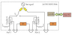
The VNA offers a cost-effective alternative to more traditional desktop VNAs. By transferring most of the signal processing and display requirements to a PC or laptop computer, the overall cost of the hardware is significantly reduced. In addition, the instrument uses a novel VNA architecture (Fig. 1) with only two receivers—rather than the customary three or four receivers—without significant loss of performance compared to full-sized (and full-priced) commercial VNA systems. The PC-based VNA achieves a dynamic range to 120 dB across a frequency range of 300 kHz to 8 GHz. It tunes with 10-Hz frequency resolution with sweep speeds to 200 μs/point. This level of performance is suitable for implementing the intended application of a cost-effective calibration-on-PCB test method for measuring SMT components to 6 GHz.
The SMT component chosen to illustrate the implementation of the calibration-on-PCB method is a model LFCN-2500 filter from Mini-Circuits.7 This is a DC-to-2.5-GHz ceramic lowpass filter housed in an FV1206-type package. It has a 3-dB point around 3 GHz and stopband attenuation of approximately 40 dB at 4 GHz.
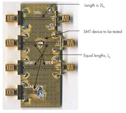
Figure 2 shows a photograph of the test jig used for the lowpass SMT filter. Apart from the SMT component to be tested, the test jig also contains all the standards needed to perform an SOLT calibration of the VNA. These are a short circuit, open circuit, near-matched load, and thru-line standard. The offset lengths of these standards are designed to achieve measurement reference planes, after calibration, which are located directly at the position of the input and output of the SMT component. Although the test jig was designed for the LFCN-2500 filter, the same approach can be used to design test jigs for other types of components.
Figure 3 shows the PCB stack-up construction for the test jig. The PCB uses four layers and has an overall finished thickness of 1.6 mm. This arrangement results in a physically rugged test jig that is able to accommodate the most widely available types of edge-launch SMA connectors.8 The width-to-height (W/h) ratio of the signal line is chosen to be 1.763, which results in a microstrip line with characteristic impedance of 50 Ω. The track width is 0.67 mm, consistent with the size of the SMT component to be tested. (The relative permittivity of the FR-4 PCB material, εr, is assumed to be 4.6.)
Apart from the microstrip lines [technically, these are grounded coplanar-waveguide (CPW) transmission lines, but the gap is large enough to make the microstrip mode dominant] on the top layer, all four layers of the test jig are grounded copper—the grounding being achieved using closely spaced interconnecting viaholes (Fig. 2). This means that only the top dielectric layer determines the impedance of the microstrip line; this, in turn, allows the 50-Ω line width to be narrow, consistent with the size of the SMT component to be tested.
This file type includes high resolution graphics and schematics when applicable.
Calibration Standards
This file type includes high resolution graphics and schematics when applicable.
It is critically important that the open, short, and load standards are connected using microstrip lines of nominally the same length (labelled Lc in Fig. 2). In addition, the nominal length of the microstrip line used to realize the thru standard must be twice the length of the line connecting the other standards (shown as 2Lc in Fig. 2). The two microstrip lines on either side of the SMT component to be tested must also have a nominal length of Lc. This commonality in line length, Lc, for the standards and the connections to the SMT component, ensures that the VNA reference planes, following calibration, are situated precisely at the terminals of the SMT component being tested.
Note: the outline of the test jig PCB has been modified (i.e., cut-away) to ensure that the thru line standard is of the correct length (2Lc). The length of the cut-away section is chosen to match the length of the SMT component being tested.
The open-circuit calibration standard is modelled as a simple fringing capacitance, with a value of 0.017 pF. This value of capacitance is established using the width-to-height ratio (W/h = 1.763) for the width of the microstrip signal line to the height (thickness) of the dielectric.9 The frequency dependence of this fringing capacitance is considered negligible at these relatively low frequencies (to 6 GHz). The short-circuit calibration standard is assumed to be perfect—i.e., with no inductance to ground—and therefore provides a complex voltage reflection coefficient of (-1, 0) at all frequencies to 6 GHz.
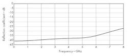
An optimally matched (50 Ω) load is the most difficult standard to realize reliably in this planar circuit (PCB) environment. Practical realization of the load typically requires testing and reworking to obtain a calibration standard with sufficiently low reflection across the frequency range of interest (in this case, to 6 GHz). A reasonable target specification for this near-matched load is to achieve a reflection coefficient of better than 30 dB, measured at the test jig’s coaxial connector.
Figure 4 shows the final arrangement used to achieve a near-matched load meeting the target specification at all frequencies. This arrangement uses two 100-Ω microwave resistors (model FC0402E 1000BSWS resistors from Vishay) connected in parallel to achieve the nominal 50-Ω terminating impedance. The lowest reflection coefficient was achieved using the mounting arrangement shown in Fig. 4.
Figure 5 shows the measured reflection coefficient for the near-matched (50 Ω) load. It reveals that the performance of the load after the effect of the edge-launch SMA connector has been removed. The load achieves very low reflection properties (i.e., a reflection coefficient of better than -35 dB to 6 GHz).
For the low-cost VNA system, the calibration kit for the measurement setup is specified by the VNA operator, using the calibration kit editor on the model LA19-13-03 VNA. For this lowpass filter example, only the open-circuit fringing capacitance must be entered. Since the test jig is a non-insertable device (it has the same sex of coaxial connectors at both ends), an adaptor was needed to realize the thru standard. The length of the thru standard was set to zero by specifying an ideal thru of zero length by means of the calibration kit editor.
Although the thru standard on the test jig does not have zero length, its length was set to zero to move the VNA reference planes to the mounting pads of the SMT component during the measurements. After defining the calibration standards on the test jig, the calibration procedure simply involves connecting each standard in turn to the ports of the VNA (Fig. 6).
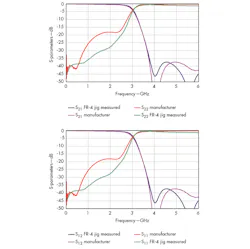
Having performed the calibration using the standards on the PCB, measurements of the LFCN-2500 lowpass filter mounted on the same PCB test jig can now be performed. The measurement results can be saved as a graphics file or as a data file in a format that can be used subsequently by a circuit simulator or read in by a spreadsheet program. Figure 7 shows the measured S-parameters (magnitude) for the lowpass filter. The measured data shows good agreement with the manufacturer’s datasheet for this device, particularly around the important regions near the 3-dB cut-off point and beyond.7
The accuracy of the LA19-13-03 VNA was verified by comparing measurement results against an independent reference. In this case, the independent reference was provided by the United Kingdom’s (UK’s) National Physical Laboratory (NPL), which is the UK’s primary measurement standards laboratory. Measurements of a 40-dB attenuator and a 25-Ω mismatch line from a 3.5-mm coaxial verification kit from Agilent Technologies were compared.10 In this measurement comparison, the NPL Primary Impedance Microwave Measurement System (PIMMS)11,12 uses a different VNA and different calibration technique.
As an example, Fig. 8 shows the results obtained for the forward reflection coefficient (S11) of the 25-Ω mismatch line. Although the measured values vary considerably with frequency (as is expected for this type of line), results obtained by the LA19-13-03 VNA show very good agreement with the NPL reference values. In fact, the two traces on Fig. 8 are superimposed, making it difficult to see the NPL results on this graph.
Similarly, Fig. 9 shows the results obtained for the forward transmission coefficient (S21) of the 40-dB attenuator. On this occasion, a very sensitive scale (40 dB ± 0.5 dB) was used to show any differences between the LA19-13-03 VNA results and the NPL results. Once again, differences were small—less than 0.06 dB at all frequencies across the band.
Similar good agreement between the LA19-13-03 VNA and the NPL reference data was obtained for the reverse reflection (S22) and reverse transmission (S12) coefficients of both test devices and for the phase of all S-parameters of both devices. This helps verify the measurements made using the LA19-13-03 VNA.
The key challenge in implementing this calibration-on-PCB technique is in realizing reliable and accurate calibration standards, particularly the near-matched load. However, with some careful design, it is possible to achieve good results, even when using low-cost FR-4 PCB substrate material for the test jig.
This file type includes high resolution graphics and schematics when applicable.
Acknowledgment
This file type includes high resolution graphics and schematics when applicable.
Nick Ridler’s involvement with this work was funded by the European Metrology Research Programme (EMRP) Project SIB62 “HF-Circuits”. The EMRP is jointly funded by the EMRP participating countries within EURAMET and the European Union.
Nils Nazoa, Director
LA Techniques Ltd., Unit 5, Chancerygate Business Centre, 214 Red Lion Rd., Surrey KT6 7RA, UK; +44 (0) 208 397 3150, Fax: +44 (0) 208 397 5372
Nick Ridler, Principal Research Scientist
National Physical Laboratory, Hampton Rd., Teddington, Middlesex, UK TW11 0LW; 020 8977 3222
References
1. J.P. Dunsmore, Handbook of Microwave Component Measurements, with Advanced VNA Techniques, Wiley, New York, 2012.
2. V. Teppati, A. Ferrero, and M. Sayed, Eds., “Modern RF and Microwave Measurement Techniques,” Cambridge University Press, New York, 2013.
3. R. A. Bauer and P. Penfold, Jr., “De-embedding and Unterminating,” IEEE Transactions on MTT-22, No. 3, March 1974, pp. 282-288.
4. A. Ferrero and U. Pisani, “Two-port network analyzer calibration using an unknown ‘thru,’ ” IEEE Microwave Guided Wave Letters, Vol. 2, No. 12, 1992, pp 505-507.
5. K. Wong, “The ‘unknown thru’ calibration advantage,” Proceedings of the 63rd ARFTG Microwave Measurement Conference, Fort Worth, TX, June 2004.
6. LA Techniques Ltd., LA19-13-03 8 GHz VNA.
7. Mini-Circuits, Brooklyn, NY, model LFCN-2500 lowpass filter data sheet.
8. Available from suppliers such as RS Components, stock number 526-5757.
9. K.C. Gupta, R. Garg, I. Bahl, and P. Bhartia, Microstrip Lines and Slotlines, 2nd ed., Artech House, Norwood, MA, 1996.
10. Agilent Technologies, Palo Alto, CA, model 85053B 3.5-mm verification kit.
11. N.M. Ridler, “A review of existing national measurement standards for RF and microwave impedance parameters in the UK,” IEE Colloquium Digest, No 99/008, pp. 6/1-6/6, February 1999.
12. N.M. Ridler, “News in RF impedance measurement,” XXVIIth General Assembly of the International Union of Radio Science (URSI), paper No 437, session A1, Maastricht Exhibition and Congress Centre (MECC), The Netherlands, August 2002.
This file type includes high resolution graphics and schematics when applicable.
About the Author

Leaders relevant to this article:


