Design A Double-Layer Shield
Double-layer shields are effective tools for achieving electromagnetic compatibility (EMC) in a wide range of high-frequency circuits. To better understand the capabilities of a double-layer shield, the shielding effectiveness (SE) of this type of shield was evaluated by modifying its geometric parameters; also altered were the electromagnetic (EM) parameters of the filling between the two shield layers. From numerical analysis—with results presented by means of the finite-difference time-domain method (FDTD)—it can be concluded that increasing the distance between the two layers, along with shifting the slot on one plate from the face-to-face position, will both bring improvements in SE. On the other hand, filling the space between the two shield layers with conductive materials decreases the SE. Some of the findings in this report may prove helpful to those attempting to apply double-shielded structures to improve the shielding in their electronic designs.
Electronic enclosures often incorporate apertures for ventilation, although the presence of these openings can compromise the shielding integrity of the enclosure. To reduce any EM transmission through these apertures, as well as their susceptibility to electromagnetic interference (EMI), double-layer shields are often employed.1,2 As a means of analyzing the SE of a particular shielding structure, the FDTD method is not only an efficient means of solving Maxwell’s equations, but a single and efficient method for predicting the SE of that structure.
In this report, the FDTD method will be used to examine double-layer shields with different geometric parameters and different filling materials between the two layers. A number of different physical parameters will be studied, such as the distance between the two layers. It was found that the SE improves linearly as the distance between the two shielding layers increases. Changes in the SE will also be studied as the slot on the external layer is shifted in the x and y directions, respectively. Numerical analysis will show that the SE improves dramatically as the slot on one layer is shifted from the face-to-face position. Finally, the effects of the filler materials between the two shielding layers will be studied for their impact on SE.
The use of conductive materials as filler will decrease the SE of the double-layer shield, while employing other materials will have only minor influence on the SE of the double-layer shield. By combining the findings of this double-layer-shield analysis, it should be possible to develop a structure with optimal SE performance.
1. (a) This diagram was used as the basis for the 3D computational model of the double-layer shield, using the configurations (b) in the x-z and (c) the y-z planes, with the changes in the distances according to the range of values shown.
The diagram in Fig. 1(a) shows a three-dimensional (3D) computational model of a double-layer shield. The model allowed studying the EM scattering from two parallel metal plates—an internal and external plate, each with the same-size slots on each plate. The internal metal shield plate is set at a distance, z, of 60 mm, while the external metal shield plate is a distance, d (in mm), from the internal plate at the source side. The source plane is 30 mm from the internal metal plate. The slots on the two plates have the same size, with slot length (L) of 60 mm and slot width (w) of 5 mm; the internal slot is located at the center of the plate. The plates are illuminated by a normal incident, z-polarized Gaussian plane wave in the form of:A total-field/scattered-field formulation (TF/SF)3 was used to implement the source, and the penetrating electric-field component, Exp, is monitored at the center of the reference plane. The latter is 75 mm from the internal shield plate at the shadow side of the double-layer shield structure. Convolution perfectly matched layer (CPML) absorbing boundary conditions4 were used to truncate the computational domain. Cubic FDTD cells 0.33 mm on a side were used in the present study, with a time step of 0.128 ps.
The actual shielding qualities to be computed throughout this report include the electric-field SE, which is given by Eq. 2:
To analyze the behavior of the double-layer shield, the position of the internal plate and the slot on the internal plate are kept constant, while the position of the external plate and the slot position on the external plate are varied. The SE is calculated at the same observation point. Software has been written based on the Fortran 95 programming language to perform this type of analysis on double-layer shields. For the present analysis, the effects of the distance between the two shielding layers on the SE were studied, as well as how the SE is impacted by the position of the slots on the two plates. The effects of the filling material’s EM parameters—such as conductivity and relative dielectric constant—on the SE of the double-layer shield were also analyzed.
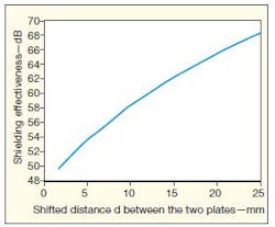
To analyze the effect of the distance between the two layers on the SE, the distance d between the double-layer shield was shifted from d = 1.67 mm to d = 25 mm. In this analysis, the two slots were located at the center of the two layers (a = 0, b = 0), and nothing is filled between the two layers. The penetrating electric-field component at the monitoring point and the SE for the double-layer shield with changing distance, d, between the two shielding plates, were analyzed and plotted in Fig. 2. As the plot shows, it is clear that the SE improves linearly as the distance between the two shielding layers increases. Thus, in a double-layer shield design, the two layers should be located as far from each other as possible.
2. This plot shows how the SE changes as a function of the distance, d, between the two shield layers.
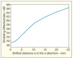
To better understand the influence of the position of the slots on the SE of the double-layer shield, the slot on the internal plate is assumed to remain constantly in the center of the plate. Meanwhile, the slot on the external plate is shifted in the x and y directions, respectively, as shown in Figs.1(b) and 1(c). In this analysis, the distance between the two plates is d = 1.67 mm, and nothing is filled between the two layers. The position of the slot is first moved by fixing the value of b at b = 0 mm while a is changed from a = 0 mm to a = 15 mm. As these values were changed, the penetrating electric-field component was analyzed at the monitor point; the results are shown in Fig. 3 with SE plotted as a function of the changing distance a. It is clear that the SE of the double-layer shield is improved as the slot on the external plate is shifted from the face-to-face position in the x direction.
3. The SE increases as the distance, a, in the x-direction increases between the two slots in the shielding layers.
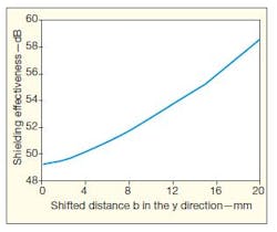
Then, with the x-direction position (a) of the slot on the external plane kept constant (a = 0), the y-direction position (b) of the slot was shifted from b = 0 mm to b = 25 mm. The penetrating electric-field component was then analyzed at the monitor point with the changing b position; the results are shown in Fig. 4 with SE plotted as a function of the changing distance b. It is clear that the SE of the double-layer shield increases steadily as the slot on the external plate is shifted from the face-to-face position in the y direction.
4. The SE increases as the distance, b, in the y-direction increases between the two slots in the shielding layers.
From this analysis, it is apparent that the SE of the double-layer shield improves as the slot is shifted in either axis from the nominal face-to-face position. To optimize the SE of the double-layer shield design, the slot on one layer should be shifted as far as possible from the face-to-face position.
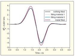
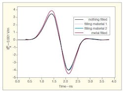
To analyze the influence of the filling material on the SE of the double-layer shield, three conditions were analyzed: with no filler, with filling material number 1, and with filling material number 2. The spacing configuration for the double-layer shield was d = 1.67 mm, a = 0 mm, and b = 0 mm. The EM parameters of filling material number 1 were conductivity, σr = 0.005 S/m; relative permittivity, εr = 2.6; and relative permeability, μr = 1.0. The EM parameters for filling material number 2 were εr = 30 S/m; εr = 1.0; and μr = 1.0. The case where metal (conductor) is filled between the two shielding layers will also be studied. The waveforms of the penetrating electric-field component at the monitor point were then compared, under circumstances when different filling materials are used and when nothing is filled between the two shield plates. Figure 5 shows the results.
5. These curves show that various filling materials, or even no filling material, have little effect on the penetrating electric-field component through the double-layer shield, but a metal conductor used as filler will decrease the SE of the double-layer shield.
As can be seen from Fig. 5, the waveforms of the penetrating electric-field component are nearly the same when material number 1, number 2, or nothing is used as filling. When metal is used as a filling material, a 1.0-dB SE is diminished. So, if a conductor, such as the metal, is used as a filler, the SE of the double-layer shield will be decreased. But if other or no filling materials are used between the layers, the effect on the SE is minimal. From this analysis, it is clear that the space between the two shielding layers should not be filled with metal or any conductive material.
In summary, from the various analyses performed with the help of the FDTD method, the importance of different shield geometrical parameters and filler materials on the SE was studied and several conclusions were drawn. As the distance between the two shielding layers of a double-layer shield increases, the SE also increases. For this reason, the two shielding layers of a double-layer shield should be separated as far apart as possible.
In addition, the SE of the double-layer shield increases as the slot on the external plate of the shield is shifted from its nominal face-to-face position. For optimum SE, the slot on one plate should
be shifted from this face-to-face position as much as possible. Using filling material between the shielding layers has little effect on SE, unless the filler is a conductive material, which will diminish the SE.
Run Xiong, Ph.D. Candidate
Bin Chen, Professor
Bihua Zhou, Professor
Yunfei Mao, Ph.D. Candidate
National Key Laboratory on Electromagnetic Environment and Electro-Optical Engineering, PLA University of Science and Technology, Nanjing, 210007, Jiangsu, China +86-2584077386 (Run Xiong), e-mail: [email protected].
References
1. J.-F. Kiang, “Shielding effectiveness of single and double plates with slits,” IEEE Transactions on Electromagnetic Compatibility, Vol. 39, 1997, pp. 260-264.
2. Y.P. Su, X. Liu, and S.Y. (Ron) Hui, “Extended theory on the inductance calculation of planar spiral windings including the effect of double-layer electromagnetic shield,” IEEE Transactions on Power Electronics, Vol. 23, 2008, pp. 2052-2061.
3. K. Umashankar and A. Taflove, “A Novel Method to Analyze Electromagnetic Scattering of Complex Objects,” IEEE Transactions on Electromagnetic Compatibility, Vol. EMC-24, No. 4, Nov. 1982, pp. 397-405.
4. J.A. Roden and S.D. Gedney, “Convolution PML (CPML): An efficient FDTD implementation of the CFS-PML for arbitrary media,” Microwave and Optical Technology Letters, Vol. 27, 2000, pp. 334-339.
