This file type includes high resolution graphics and schematics when applicable.
Advanced modulation formats, such as very-minimum-chirp-keying (VMCK) modulation, can provide extremely high bandwidth efficiency when high data rates are desired for limited available bandwidths. To better understand the use of VMCK modulation, it can be useful to develop transmission models for a system’s transmitter and receiver, using field-programmable gate arrays (FPGAs) to implement the design.
Increasing demands for higher wireless data rates highlight the limited radio spectrum resources available—for instance—in Fourth-Generation (4G) mobile communications systems.1-3 To achieve effective use of available bandwidth, efficient modulation schemes are needed. For example, very-minimum-shift-keying (VMSK) modulation and demodulation with extremely high bandwidth efficiency was first proposed in 1997.4 In 2001, very-minimum-waveform-difference-keying (VWDK) modulation was proposed in which minimum different sinusoidal waves were used to modulate the binary information.5
In 2007, VMCK modulation was proposed in which binary data is formed by raising or reducing the frequency in one bit period.6 Since then, modulation schemes with higher bandwidth efficiencies have been investigated.7-10
To study the modulation and demodulation of VMCK signals, it can be helpful to design a hardware platform based on an FPGA. In the transmitter, the VMCK signal are generated by means of the integrated software environment (ISE) from Xilinx, Inc. running on a personal computer (PC). The digital VMCK signals from the FPGA output are then converted to analog VMCK signals by means of digital-to-analog-converter (DAC) circuitry. RF-modulated VMCK signals will then be transmitted via an RF demodulation module.
In the receiver, which includes RF demodulation, synchronization circuit, analog-to-digital-converter (ADC) circuitry, and FPGA, received RF signals are converted to baseband analog signals via RF demodulation. The synchronization module’s function is to initialize signals on the bit synchronization rising edge. Sampled data of VMCK analog signals output from the ADC circuitry are regarded as inputs to the FPGA. The FPGA module obtains the final demodulation data stream at the output of the comparator, where the result is compared against a predefined threshold.
VMCK modulation is a novel communication scheme with extended application of chirp signal characteristics. VMCK signals can be defined by Eq. 1:
sN(t) = n∑k = - ∫[1 + IeαN - 2IeαNf5(t - kT)]sin[2πNf5[1 + IeαNf5(t - kT)](t - kT)
0 < αN ≤ 1, nT ≤ t ≤ (n + 1)T (1)
where:
sN(t) represents data 0 or 1, when Ie = -1 or Ie = 1;
N is the number of the signal period;
fs is the frequency of the signal at the middle of the digital bit and is equal to the bit transmission rate; and
αN is the chirp modulation factor.
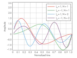
Figure 1 shows VMCK waveforms for one and two periods, with N = 1 and α1 = 0.696 and N = 2 and α2 = 0.36.
If Ie = -1 and N = 1, then:
sV0(t) = (1 - α1 + 2α1fst)sin[2πfs(1 - α1 + α1fst)t], 0 < α1 ≤ 1, 0 < t ≤ T (2)
If Ie = 1 and N = 1, then:
sV1(t) = (1 + α1 - 2α1fst)sin[2πfs(1 + α1 - α1fst)t], 0 < α1 ≤ 1, 0 < t ≤ T (3)
where sv0 and sv1 represent data 0 and 1 states, respectively.
Equations 2 and 3 portray VMCK signals for a single period. The integrated values of sv0(t) and sv1(t) are equal to zero in one symbol period. The VMCK signals are easily demodulated at the receiver by eliminating direct current offset. A transmission model of the VMCK modulated signals is shown in Fig. 2.
The VMCK modulated signal, sin(t), is first passed through an additive white Gaussian noise (AWGN) channel, represented by Eq. 4:
s(t) = sin(t) + n(t) (4)
The noisy signal, s(t), is then processed by a bandpass filter (BPF):
s'(t) = s(t) * h(t) (5)
where the * represents convolution. The filter is designed to satisfy passband and stopband requirements, and the filtered signal, s'(t), must carry most modulated signals’ energy to ensure reliable signal transmission.
The filtered signal, s'(t), is demodulated by a two-path multiplier and integrator (Eqs. 6 and 7):
s'0(t) = (1/f)∫0 s'(t)[ s'0(t) * h(t)]dt (6)
s'1(t) = (1/f)∫0 s'(t)[ s'1(t) * h(t)]dt (7)
Finally, the demodulated data stream is obtained at the output of the comparator, where the integration result is compared against a predefined threshold.
s'1(t) - s'0 ≥ 0 → sout(t) = 1 (8)
s'1(t) - s'0 < 0 → sout(t) = 0 (9)
This file type includes high resolution graphics and schematics when applicable.
A Closer Look
This file type includes high resolution graphics and schematics when applicable.
Figure 3 presents the structure of the VMCK transmitter, which is comprised of an FPGA, DAC, and RF modulation block. VMCK signals are generated by means of ISE on the PC. The data sequence “101010…” is fed into the FPGA, where the VMCK modulation is carried out. Figure 4(a) shows the output signal waveform of the most significant bit (MSB) in the FPGA’s 8-b output data, for a signal frequency of 2 MHz.
The duty ratio of the loop “10” VMCK waveform is reflected in Fig. 4(a). The VMCK digital signal is converted to a VMCK analog signal in the DAC according to the sampling clock from the FPGA, as shown in Fig. 4(b), where the repeating pattern “10” can be observed.
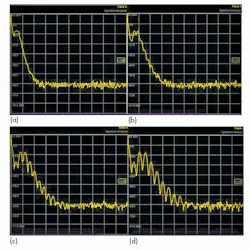
Spectra for VMCK analog signals with different center frequencies (2, 3, 4, and 5 MHz) can be seen in Figs. 5(a-d). The energy of these VMCK signals is concentrated around each center frequency, with 90% signal energies occupying 20%, 30%, 40%, and 50% bandwidths for the 2-, 3-, 4-, and 5-MHz center frequencies, respectively. The signal spectra grows broader with increasing center frequency. Such RF modulated analog VMCK signals are then transmitted.
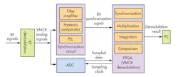
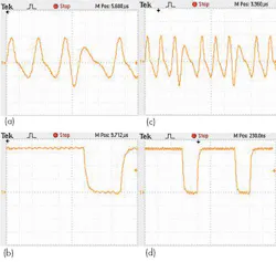
Figure 6 shows the VMCK receiver design, which includes an RF demodulation block, synchronization circuits, ADC, and FPGA. RF signals are first converted to analog baseband signals via the RF block. Analog baseband VMCK signals are applied to both the ADC and synchronization circuits. The ADC converts sampled analog VMCK signals into 8-b digital signals, which are then fed to the FPGA. Figure 7(a) is a waveform of the MSB of the ADC’s 8-b output.
The synchronization circuit includes filter amplifier, hysteresis comparator, and phase-locked loop (PLL). The filter amplifier filters off the center frequency of the baseband signal. The hysteresis comparator is designed to compare the input level with a reference level. If an input level is greater than the reference level, the output is low, and if the input level is less than the reference level, the output is high.
The PLL circuit includes a phase detector, loop filter, and voltage-controlled oscillator (VCO). The synchronization circuit obtains the center frequency of the baseband signal, and the PLL circuit locks in a square wave of this frequency, thus providing a bit synchronization signal to the FPGA. Figure 7(b) shows the bit synchronization signal.
The FPGA demodulation module includes synchronization, multiplication, integration, and comparison modules to implement coherent demodulation. The synchronization module’s function is to initialize on the bit synchronization rising edge. The multiplication module’s output is each multiplication operation result within each sampling time.
The integration module implements the accumulation operation of the multiplication module’s output in one symbol period. The demodulated data stream is obtained at the output of the comparator, and the integration result is compared against a predefined threshold. Figure 7(c) shows demodulation for a loop “10” VMCK waveform, with the correct demodulation result being approximately square waves.
To further test the VMCK transmission system, a loop “1110” sequence can be sent by the transmitter. For example, Fig. 8(a) shows the transmitted sequence “11101,” with the demodulation result of “11101” shown in Fig. 8(b). Figure 8(c) shows the transmitted sequence “1110111011” and Fig. 8(d) provides the demodulation result of “1110111011.” Both tests are correct. The model of the VMCK system helps portray the basic principles of this novel transmission approach, including the use of FPGA models.
Acknowledgments
This work is supported by Shanghai Leading Academic Discipline Project Nos. S30108, NSFC 61132003, and NSFC 61171086.
Liu Yang, Ph.D. Candidate
Guoxin Zheng, Professor and Team Leader of Wireless Communication
Zhongpin Luo, Postgraduate Student
School of Communication and Information Engineering, Shanghai University, Shanghai, Baoshan, People’s Republic of China
References
1. J. Browne, “Channel Emulator Exercises MIMO,” Microwaves & RF, Vol. 50, No. 4, 2011, pp. 104-104.
2. J.H. Kim, M. Younis, A Moreira, et al., “A Novel OFDM Chirp Waveform Scheme for Use of Multiple Transmitters in SAR,” IEEE Geoscience and Remote Sensing Letters, Vol. 10, No. 3, 2013, pp. 568-572.
3. M.N. Seyman and N. Taspinar, “Channel estimation based on neural network in space time block coded MIMO-OFDM system,” Digital Signal Processing, Vol. 23, No. 1, 2012, pp. 275-280.
4. H.R. Walker, “VPSK and VMSK modulation transmit digital audio and video at 15 bits/sec/Hz,” IEEE Transactions on Broadcasting, Vol. 3, No. 1, 1997, pp. 96-103.
5. K.H. Saywood, Lenan Wu, “Raise bandwidth efficiency with sine-wave modulation VMSK,” Microwaves & RF, Vol. 40, No. 4, 2001, pp. 79-84.
6. Guoxin Zheng, Jinzhen Feng, and Minghua Jia, “Very Minimum Chirp Keying as a Novel Ultra Narrow Band Communication scheme,” ICICS, 2007, pp. 1-3.
7. Liu Yang, Guoxin Zheng, Yabin Li, and Xing Sun, “Performance analysis of UNB modulation based on VMCK in AWGN channel,” IET CCWMC, 2011, pp. 207-210.
8. Man Feng, Lenan Wu, and Jiajia Ding, “BER analysis and verification of EBPSK system in AWGN channel,” IEICE Transactions on Communications, Vol. E94B, No. 3, 2011, pp. 806-809.
9. Shikai Zhang, “Assessing Different Ultranarrowband Formats,” Microwaves & RF, Vol. 51, No. 8, 2012, pp. 76-79.
10. Liu Yang, Guoxin Zheng, Qingfeng Ding, et al, “Optimal Design of VMCK High-Order BPF,” Journal of Cases on Information Technology (JCIT), Vol. 8, No. 1, 2013, pp. 512-520.
This file type includes high resolution graphics and schematics when applicable.
About the Author
Liu Yang
Guoxin Zheng

Leaders relevant to this article:


