Mixer Translates Multiple Standards
Wireless communications products continue to support multiple communications standards, pushing designers to develop components that can work across as many bands and standards as possible. Ideally, a single device would handle all wireless communications standards and bands. But before that day comes, it is necessary to develop components—such as upconversion mixers—that can operate with several wireless standards. By employing a cross-coupling post-distortion technique (CCPFT), it was possible to design an upconversion mixer with outstanding linearity for multiple wireless communications standards.
The mixer was simulated with commercial software, based on fabrication with a CHRT 0.18-μm silicon CMOS mixed-signal/RF semiconductor process. As will be shown, the mixer consumes only 5 mW power from a +1.2-VDC supply. It achieves a maximum input third-order intercept point (IIP3) of +16.56 dBm with 3.5 dB conversion gain (flat to within ±0.5 dB), with 10.7-dB noise figure (flat to within ±0.5 dB) across a frequency range of 1.0 to 10.6 GHz. This makes it ideally suited for software-defined radios (SDRs), as well as multiple-band ultrawideband (UWB) communications systems.1
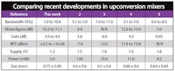
An upconversion mixer should provide low noise figure with reasonable gain and high linearity while consuming low power to be effective in modern multiple-standard wireless transmitters. Such mixers have been developed, including the 3.0-to-5.1-GHz upconversion mixer of ref. 2 designed with a current-reuse technique to minimize power consumption. It delivers 3.8-dB gain and 8.4-dB noise figure, but only −7.6-dBm IIP3. In ref. 3, a 1.0-to-11.0-GHz upconversion mixer was proposed, with an adopted fold structure and inductor-free matching network. Although its IIP3 reaches +12 dBm, the conversion gain is below 0 dB (−6 dB).
In ref. 4, a 3.0-to-5.0-GHz upconversion mixer with current-reuse bleeding technique was presented. It achieves 6.5-dB conversion gain and IIP3 of +11.6 dBm. However, its power dissipation is 11.0 mW, and the mixer has a very complicated structure. In ref. 5, a 6.0-to-8.0-GHz upconversion mixer was proposed which uses a feedback loop in its transconductance stage. It achieves 0-dB conversion gain and 7.0 dB noise figure, but its linearity is not mentioned. From these reference examples, it is apparent that tradeoffs were made between linearity and other performance parameters.
For high upconversion-mixer linearity without sacrificing the other key mixer performance parameters, it is necessary to apply some linearization techniques. Numerous circuit linearization techniques have been developed for low-noise amplifiers (LNAs). One commonly used method is the derivative superposition technique.6,7 It employs auxiliary transistors biased via weak inversion, which produces a nonlinear current to cancel out the third-order intermodulation generated by the main transistors. This approach is mainly effective at lower frequencies and can induce additional gate noise. Recently, a post-distortion technique8 and a cross-coupling post-distortion technique9,10 were implemented for LNA linearization. Both methods yielded IIP3 performance levels exceeding +10 dBm without seriously degrading the other key LNA parameters.
For multiple-standard wireless communications applications, a low-voltage upconversion mixer was developed using a pseudodifferential double-balanced structure, allowing for high isolation between ports while operating with low supply voltage. It also employs a current-bleeding topology for improved noise and linearity performance.11 A cross-coupling post-distortion technique was also adopted to further improve IIP3. The added linearization circuitry does not increase the size of the mixer, nor does it degrade conversion gain, noise figure, or power consumption.
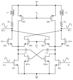
Figure 1 shows a schematic circuit diagram for the UWB multiple-standard mixer, with a structure that is an improvement over a Gilbert-cell double-balanced mixer. Transistors M1 and M2 comprise the input pseudo-differential transconductance pairs. Transistors M1a and M2a employ weak inversion biasing. They form the cross-coupled post-distortion structure, which generates the nonlinear current needed to cancel the third-order intermodulation distortion generated by M1 and M2. Capacitors C1 and C2 are coupling capacitors, while transistors M3, M4, M5, and M6 work as switches. Transistors M7 and M8 serve as current sources to improve the noise and linearity performance of the whole circuit by adjusting the bias current. Resistors R1 and R2 are load resistors, while inductors L1 and L2 are useful for increasing the conversion gain at the upper edge of the desired frequency range.
The linearity of a Gilbert-cell mixer is determined mainly by its transconductance stage.12 As a result, post-distortion linearization is implemented on the pseudo-differential transconductance stage (Fig. 2). To explain the basic operating principle of this approach, reactive components must be ignored in this analysis and all device pairs considered to be without mismatches. Then the drain current of each transistor can be represented as a power-series expression, with a gated-source voltage provided by transistors. For simplicity, the output current, iout+ of the left half-circuit composed of transistors M1 and M1a is considered first. The drain currents of those two transistors can be modeled as Eqs. 1-4:
where:
RON = the switch on resistance of the switch pair;
a = RONg1;
b = RONg2; and
c = RONg3;
The two nonlinear currents i1 and i1 a add at node v3, yielding output current iout+:
The third-order derivative g3 in Eq. 1 is a dominant source of third-order intermodulation distortion, which limits the linearity of a mixer. To improve the linearity, g3 should be minimized without reducing the fundamental transconductance, g1. The differential transistor pair M1 and M2 is biased in strong inversion, which has a negative third-order derivative g3. Therefore, the third-order nonlinearity provided by the cross-coupling post-distortion canceller FET should be positive, which requires biasing FETs M1a and M2a in the weak inversion region. From Eq. 5, it can be seen that current i1a partially cancels both the second- and third-order terms of current i1.
A time-varying Volterra series can be used at high frequencies to analyze the high-frequency inter-modulation performance of the proposed mixer. The mixer’s distortion is induced by the switching and transconductance stages. Reference 12 provides a detailed analysis of the intermodulation distortion of the switching pairs. The effectiveness of the applied linearization is determined mainly by the transconductance stage. For simplicity in this analysis of the mixer, distortion due to the switch pairs has been neglected. The parasitic capacitance and resistance of two auxiliary transistors, except the gate-source capacitance, have also been ignored in the analysis. Figure 3 shows a version of the mixer schematic diagram for use in high-frequency distortion analysis. This is limited to a third-order analysis, assuming a weakly nonlinear circuit. The expression for IIP3 is given by a Volterra series analysis as follows13:
where:
where:
ZM = the equivalent impedance of the switch transistor and
ZL = the equivalent impedance of the load.
Equations 9 through 16 imply that the mixer’s linearity (IIP3 or OIP3) is determined by g1`, g3`, and gOB. Parameter gOB represents the combined effect of the second-order nonlinearity generating the second-order intermodulation product, which is then mixed with the fundamental tones, yielding the third-order products.13 This self-interaction is due to the multiple feedback in the circuit mainly by the gate-drain capacitance.13
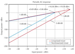
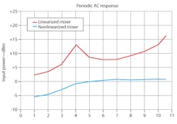
From Eqs. 12-15 it can be shown that the values of |H(ω)|, |A1(ω)|, and |ε(Δω, ω1 + ω2)| decrease when the cross-coupling post-distortion technique is implemented in the Gilbert-cell mixer. For this reason, the proposed mixer achieves higher linearity than a double-balanced mixer using a traditional current-bleeding technique. The analysis for the proposed mixer can be confirmed by simulation results shown in Figs. 7 and 8.
Noise at the output of the upconversion mixer is caused mainly by the channel thermal noise and the flicker noise of the transconductance stage, and the thermal noise generated in the switching pair and the load.
Because the noise from a transistor is proportional to its transconductance, the noise contribution from the auxiliary transistor is very small and can be neglected in an analysis. The noise figure of the proposed upconversion mixer can be calculated by Eq. 1714:
where the quantities α, c, G, and G2 are evaluated with the bias current of each switch pair and symbols γ1 and γ5 represent noise factor γ for transistors M1 and M5, respectively. Parameter K is a coefficient used in the analysis.
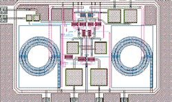
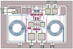
Computer simulations on the upconversion mixer were performed with the aid of the Cadence Spectre program from Cadence Design Systems (www.cadence.com) and using the CHRT 0.18-µm mixed-signal/RF CMOS process from Singapore’s Chartered Semiconductor Manufacturing Ltd. Figure 4 shows a layout of the upconversion mixer, which occupies an area of 0.75 × 0.5 mm.
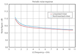
It was evaluated with local-oscillator (LO) input power of +1 dBm, intermediate-frequency (IF) input power of −30 dBm, with the IF fixed at 10 MHz and the LO frequency swept from 1.0 to 10/.6 GHz. The simulated conversion gain was found to be within ±0.5 dB of 3.5 dB, as shown in Fig. 5. For the noise figure shown in Fig. 6, the IF was also fixed at 10 MHz and the LO frequency swept from 1.0 to 10/.6 GHz, with the simulated results showing noise figure of better than 10 dB across most of the frequency range.
Figure 7 shows simulated IIP3 versus RF output frequency. At 10.61 GHz, the simulated IIP3 performance is +16.56 dBm. For Fig. 8, the IIP3 is shown across the full RF range, with the LO frequency swept from 1.0 to 10.6 GHz. The table summarizes the performance of the proposed upconversion mixer, comparing it to other reported mixers. The mixer proposed here achieves higher linearity than these other mixers, with lower operating voltage.
In summary, the simulations for an upconversion mixer based on a commercial 0.18-µm CMOS process show good results when applying a post-linearization technique to enhance linearity at low voltage levels. The mixer, which draws only 5 mW power from a +1.2-VDC supply achieves peak IIP3 of +16.56 dBm while also providing conversion gain of 3.5 dB. It is designed for use from 1.0 to 10.6 GHz and is suitable for multiple-standard wireless and UWB communications applications.
Acknowledgments
The authors would like to thank the Science and Technology Planning Project of Hunan Province No.2010FJ4246 and the Fundamental Research Funds for the Central Universities NO.531107040269 for financially supporting this research.
References
1. S.S.K. Ho and C.E. Saavedra, “A CMOS Broadband Low-Noise Mixer With Noise Cancellation,” IEEE Transactions on Microwave Theory and Techniques, Vol. 58, No. 5, May 2010, pp. 1126-1132.
2. Giuseppia Sapone and Giuseppe Palmisano, “A 0.25-μm CMOS Low-Power Up-Conversion Mixer for 3.1-5 GHz Ultra-Wideband Applications,” Research in Microelectronics and Electronics, Ph.D. disseration, September 2006, pp. 457-460.
3. Pin-Cheng Huang, Fong-Cheng, et al., “A Miniature, Folded-Switching, Up-conversion Mixer for UWB Applications Using 0.18-μm CMOS Process,” 2007 IEEE Radio Frequency Integrated Circuits Symposium, September 2007, pp. 501-504.
4. Wen-Shan Hxiao and Zhi-Ming Lin, “A 1-V, 11.6-dBm IIP3 Up-Conversion Mixer for UWB Wireless System,” 52nd IEEE International Midwest Symposium on Circuits and Systems, August 2009, pp. 1042-1046.
5. Dalenda Ben Issa, Abdennaceur Kachouri, and Mournir Samet, “Design And Optimization of Up-Conversion CMOS Mixer For UWB Application. 6th International Multi-conference on Systems, Signals and Devices, March 2009, pp. 1-4.
6. Jiming Jiang and D. M. Holburn, “Design and analysis of a low-power highly linear mixer,” European Conference on IEEE Circuit Theory and Design 2009 (ECCTD 2009), August 2009, pp. 675-678.
7. Tae Hwan Jin and Tae Wook Kim, “A 5.5-mW 9.4-dBm IIP3 1.8-dB NF CMOS LNA Employing Multiple Gated Transistors With Capacitance Desensitization,” IEEE Transactions on Microwave Theory and Techniques, Vol. 58, 2010, pp. 2529-2538.
8. Heng Zhang, Xiaohua Fan, and E.S. Sinencio, “A Low-Power, Linearized, Ultra-Wideband LNA Design Technique,” IEEE Journal of Solid-State Circuits, Vol. 44, No. 2, February 2009, pp. 320-330.
9. Tae-Sung Kim and Byung-Sung Kim, “Linearization of Differential CMOS Low Noise Amplifier Using Cross-Coupled Post Distortion Canceller,” 2008 IEEE Radio Frequency Integrated Circuits Symposium, June, 2008, pp. 83-86.
10. Gholamreza Zare Fatin, Ziaddin Daei Koozehkanani, and Henrik Sjoland, “A 90-nm CMOS +11 dBm IIP3 4 mW Dual-Band LNA for Cellular Handsets,” IEEE Microwave and Wireless Components Letters, Vol. 20, No. 9, September 2010, pp. 513-515.
11. Farid Touai, Skandar Douss, and Mourad Loulou, “A 0.35-μm CMOS Mixer for 3.1-4.8 GHz UWB MB-OFDM Receivers,” 14th IEEE International Conference on Electronics, Circuits and Systems, December 2007, pp. 1220-1223.
12. Manolis T. Terrovitis and Robert G. Meyer, “Inter-modulation Distortion in Current-Commutating CMOS Mixers,” IEEE Journal of Solid-State Circuits, Vol. 35, No. 10, October 2000, pp. 1461-1473.
13. Bonkee Kim, Junb-Su Ko, and Kwyro Lee, “Highly Linear CMOS RF MMIC Amplifier Using Multiple Gated Transistors and its Volterra Series Analysis,” 2001 IEEE MTT-S International Microwave Symposium Digest, Vol. 1, pp. 515-518.
14. Manolis T. Terrovitis and Robert G. Meyer, “Noise in current-commutating CMOS mixers,” IEEE Journal of Solid-State Circuits, Vol. 34, No. 6, June 1999, pp. 772-783.
