Transceiver Supports 8 × 8 MIMO Systems
This file type includes high resolution graphics and schematics when applicable.
Modern communications systems are often judged by their data rates. Organizations such as the International Telecommunication Union (ITU) suggest by their definitions that next-generation mobile-communications systems should operate at rates to 100 Mb/s for high-mobility operation and 1 Gb/s for low-mobility operation. So far, third-generation (3G) communications networks and their more advanced successors, such as 3.5G networks, can support data rates to several megabits per second.1-4
Related Articles
• Development Software Addresses MIMO Testing
• MIMO Transceivers Aid TD-LTE Systems
• Signal Generator Simplifies Complex MIMO Tests
Of course, modern communications users will want even faster data rates as part of fourth-generation (4G) wireless networks. In China, for example, time-division, long-term-evolution (TD-LTE) wireless technology in the 2.6-GHz spectrum (2500 to 2690 MHz) using time-division-duplex (TDD) techniques offers the promise of high data rates in wireless communications.
In many ways, with its application of orthogonal-frequency-division-multiplexing/frequency-division-multiple-access (OFDM/FDMA) technology, 3GPP LTE networks have been considered “Quasi 4G” systems. In other words, they apply 4G technologies to 3G systems for improved performance, including the use of multiple-input, multiple-output (MIMO) antenna techniques. The use of these advanced technologies allow 3G networks to achieve data rates of 100 Mb/s on downlinks and 50 Mb/s on uplinks.5,6
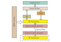
RF/microwave engineers are concerned with achieving the highest performance possible using TDD-LTE technology in these wireless networks. To aid those efforts, the current transceiver was developed as part of a project for a next-generation wireless communications system for use in radio-over-fiber (RoF) applications. The transceiver supports 8 × 8 MIMO use in user-equipment (UE) and base-transceiver-station (BTS) equipment. The transceiver’s output is designed for connection to an optical transceiver and front amplifier unit (FAU) (not included in this report). Figure 1 shows a block diagram of the full system.
Transceiver architectures typically rely on either zero-intermediate-frequency (zero-IF) or superheterodyne configurations. Zero-IF approaches have been widely used in personal mobile devices due to their low cost and practical application as single-chip devices.7,8 The current transceiver design is based on the superheterodyne approach so as to achieve maximum performance, even though it is somewhat bulky and costly.
Each transceiver consists of several main parts, including a transmitter circuit, receiver circuit, local-oscillator (LO) module, and control circuit. Figure 2 shows a simplified block diagram. The whole system operates in the TDD scheme. Therefore, a RF switch controlled by transmit/receive (T/R) switch signal ensures that the system can be switched between transmit and receive states.
The switching time must be short enough to meet the standards of TDD-LTE systems, or it may affect the first few symbols used for channel estimation. The decoupling capacitors of some key devices and the resistive-capacitive (RC) network of the RF switch should be designed carefully. The T/R switch signal is also used to control four other switches used in the transmitter and receiver circuits, maintaining high isolation between the two circuits.
In contrast to many conventional superheterodyne systems, the baseband output of this system is a 185-MHz digital IF signal. At baseband, the signal is sampled at digital IF with a higher sample rate to help avoid potential problems. A baseband anti-aliasing filter can provide much better performance in the digital domain compared to an analog filter. Of course, as digital-signal-processing (DSP) techniques have become more widely used, this superheterodyne transceiver architecture with digital IF has also grown in popularity.
This file type includes high resolution graphics and schematics when applicable.
A Closer Look
This file type includes high resolution graphics and schematics when applicable.
The transceiver’s transmitter consists of several amplifiers, an IF/RF filter, a mixer, digital attenuators, and switches. Because the signal from baseband remains constant, the transmitter’s output power is changed by means of two digital attenuators which work in conjunction with several small-signal amplifiers and one power amplifier to achieve desired transmit power levels. These components should be carefully designed to achieve the required transmit performance parameters, including output power, linearity, and spurious suppression. For example, an LTE signal must have high peak-to-average power ratio (PAPR), especially with complex modulated signals reaching 8 dB or higher. As a result, the power amplifier should be designed with such requirements in mind.
The receiver circuitry—with its low-noise amplifier (LNA) IF/RF filter, mixer, digital attenuators, switches, and small-signal amplifiers—is somewhat similar in architecture to the transmitter circuitry, differing in its dynamic range. The receiver circuitry should not only provide enough gain for small signals, but also avoid amplifier saturation for large signals. As a result, gain control is an important function for the receiver circuitry.
The gain control is achieved by means of several gain blocks and two digital attenuators for 64-dB total gain control with 0.5-dB gain control per step. The passive mixer is used to convert RF signals to the IF stage. As with the transmitter, the layout and device selection for the receiver circuitry should be carefully considered to achieve desired linearity and spurious suppression.
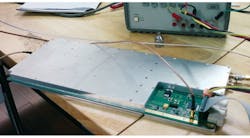
Each channel of the transceiver was designed on a four-layer FR-4-based printed-circuit board (PCB) with relative dielectric constant (εr) of 4.6 to achieve small size and low cost. System-level transceiver simulation was performed with the ADS 2009 Advanced Design System (ADS) simulation software from Agilent Technologies. To avoid possible interference between function modules, each RF board was designed and assembled with several metal compartments for isolation. This metal framework with covers was indispensable for achieving good electromagnetic-interference (EMI) shielding. Figure 3 shows one of the transceiver channels.
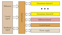
For general-purpose use, all of the transceiver’s control signals are realized by a single-chip complex programmable logic device (CPLD), and all eight transceiver channels can be controlled and synchronized separately through the backboard. The system requires a frequency synthesizer control signal and reference clock for the synthesizer’s phase lock loop (PLL). Since the quality of the reference oscillator is closely tied to the oscillator phase noise, the amplitude, waveform quality, and jitter of the reference oscillator are important parameters in the design of the overall system.
The transceiver system’s power board provides DC-to-DC conversion from +48 VDC to +6 VDC for the system. The control board acts as an interface between the baseband control signal and the RF board’s control operation. It includes power and gain control for each transmitter and receiver, respectively, along with other functions like reference clock calibration.
The reference board provides an accurate 10-MHz reference clock which is generated by an oven-controlled crystal oscillator (OCXO). A PLL circuit is carefully designed to lock and track a 30.72-MHz Global-Positioning-System (GPS) reference clock from baseband quickly, even if the OCXO has a very slight change due to an external disturbance.
The full transceiver system includes eight RF boards, one backboard, one power board, one control board, and one reference board (Fig. 4). The performance of the transceiver was evaluated with commercial test equipment from some of the top suppliers. A model N5767A power supply from Agilent, for example, provides the full system’s +48 VDC voltage, while models E4438C and N5182 signal generators and a model N9030 signal analyzer from the firm were also used in the testing.
A model FSUP50 signal source analyzer from Rohde & Schwarz, with available models to 26.5 GHz, was also used as part of the test system to check LO phase noise. The LO module is designed to provide low-phase-noise signals, providing IF LO signals at 965 MHz and RF LO signals at 1.45 GHz.
For each transmit channel, output power, linearity, and gain flatness are key performance parameters. Across the full 100-MHz bandwidth of the transmit channel, gain fluctuation is less than 1 dB. This is due to careful design and tuning to achieve optimum impedance matches between difference devices and circuit layouts, especially for the impedance match of the amplifier and filter. The maximum output power of each channels is about +23 dBm, with third-order intermodulation (IMD3) held as low as -53 dBc (tested with a two-tone signal with 1-MHz spacing). As Fig. 6 shows, each transmitter channel achieves good linearity.
This file type includes high resolution graphics and schematics when applicable.
The ACPR Approach
This file type includes high resolution graphics and schematics when applicable.
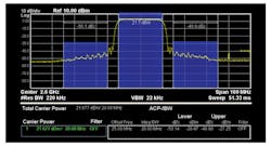
Another means of evaluating the transceiver’s linearity and spectral spreading between the main channel (useful signal) and adjacent channel (intermodulation signal) is by ACPR testing and analysis, especially in modern wireless communications systems. For output power of +23 dBm, the transceiver’s ACPR is less than -49 dBc. The evaluation was performed with 64-state quadrature-amplitude-modulation (64QAM) signals, with a reference bandwidth of 20 MHz and reference offset of 5 MHz (Fig. 7).
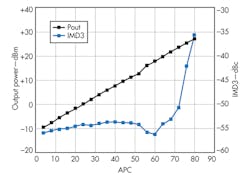
Unlike the transmit channel, the receive channel requires a stable output power level of around -10 dBm and IMD3 of better than -50 dBc for the baseband over a wide power range in spite of the power of the received signal. Gain fluctuation for each receiver channel is less than 1.5 dB in a 100-MHz bandwidth—slightly larger than that of the transmitter due to the ripple of two IF cavity filters. Still, this performance level can be tolerated since multicarrier modulation is commonly used in modern systems. It is also difficult to use a 100-MHz-bandwidth single-carrier modulation technique for TDD-LTE signals in a wireless communication system.
The error-vector-magnitude (EVM) parameter was used to appraise the whole system’s performance, since it provides information on some key system performance levels, including amplitude/phase imbalance, gain compression/flatness, and phase noise. EVM measurements were performed with the aid of a model N9030A PXI signal analyzer from Agilent and the company’s model 89600A vector-signal-analyzer (VSA) software. Due to the limits of the available test equipment, the maximum symbol rate used for testing was 20 MHz, although this was sufficient to verify system performance.
The test signals include 16QAM, 64QAM, and TDD-LTE characteristics. Characterization of the test system includes test cables with insertion loss of 3.3 dB at 2.6 GHz. The measured EVM levels for 16QAM and 64QAM signals were both less than 0.9% while the transceiver works without switching, which is excellent performance. The spectra of the transmitter and receiver deteriorate somewhat with switching, as depicted in Fig. 8 for TDE-LTE test signals.
The table summarizes the performance levels for all eight transceiver channels. The slight differences among these channels and the EVM of the transmit/receive signals is around 1.7% to 2.3%. The transceiver was tested with continuous switching between transmit and receive states under the control of the N7625B signal studio software and the E4438C signal generator.
According to the design procedure and test results, one phenomenon should be pointed out. This TDD system consists of as much as eight transceivers, and its current can fluctuate considerably when switching between transmit and receive modes. For example, the system’s current is about 13 A when the transmit state is on and 4 A when the transmit state is off. This may be a serious problem for some aspects of transceiver performance, such as phase noise.
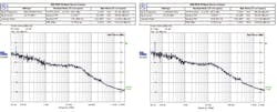
With only one +48-VDC power supply for the full system, the DC power’s current fluctuation may influence the LO module’s performance in parameters such as stability. One phenomenon is the EVM will deteriorate at a rapid pace, particularly the constellation rotation, which is an intimation of poor phase noise (Fig. 9, left). The distortion of the constellation’s magnitude is evident, such as the constellation of the QPSK signal (Fig. 9, left). This deterioration is not only related to the current fluctuations, but is also likely affected by switching speed and some other transceiver functions.
Some applications require proper decoupling and active filter circuit for each transceiver’s LO module and the reference board’s power supply has been adopted and carefully designed in this eight-channel MIMO system. According to Fig. 9 (right), which shows a TDD-LTE constellation with treated power, the EVM deteriorates seriously only during the first several symbols in less than 1 μs, and then a stable constellation is achieved. This is in sharp contrast to the EVM for untreated power (Fig. 9, left).
Acknowledgments
This work was supported in part by National 973 project 2010CB327400 and in part by the National High-Tech Project under Grant 2010ZX03007-002-01, 2011ZX03004-001. The authors would also like to acknowledge Agilent Technologies and Rohde & Schwarz for providing test instruments for the measurements.
This file type includes high resolution graphics and schematics when applicable.
References
This file type includes high resolution graphics and schematics when applicable.
1. Z.Q. Yu, J.Y. Zhou, J.N. Zhao, T. Zhao, and W. Hong, “Design of a Broadband MIMO RF Transmitter for Next-generation Wireless Communication Systems,” Microwave Journal, Vol. 53, No. 11, November 2010, pp.22-26.
2. A. Hashimoto, H. Yoshino, and H. Atarashi, “Roadmap of IMT-advanced development,” IEEE Microwave Magazine, Vol. 9, 2008, pp. 80-88.
3. Martin Sauter, Beyond 3G -Bringing Networks, Terminals, and the Web Together: LTE, WiMAX, IMS, 4G Devices, and the Mobile Web 2.0, Wiley, New York, 2009.
Related Articles
• Development Software Addresses MIMO Testing
• MIMO Transceivers Aid TD-LTE Systems
• Signal Generator Simplifies Complex MIMO Tests
4. Zhe Chen, Wei Hong, Jianyi Zhou, Jixin Chen, and Chen Yu, “Design of Miniature RF Transceivers for Broadband MIMO Systems in Ku-Band,” Microwave Journal, Vol. 55, No. 11, November 2012, p. 108.
5. Weiming Wu, Junyi Li, and Ghao Guyong, “Research of key technologies in TD-LTE system,” Global Mobile Congress 2009.
6. A. Ghosh, R. Ratasuk, B. Mondal, N. Mangalvedhe, and T. Thomas, “LTE-advanced: next-generation wireless broadband technology,” IEEE Wireless Communications, Vol. 17, No. 3, June 2010, pp.10-22.
7. Jianyi Zhou, Jianhong Chen, Jianing Zhao, Jianjun Wang, and Wei Kang, “Design of a high performance RF transceiver for WiMAX basestation,” Proceedings of the APMC, Vol. 5, December 2005, pp. 365-371.
8. Ken Hansen and Alexis Nogleras, “Receiver RF Design Considerations for Wireless Communications Systems,” IEEE Transactions on Circuits and Systems, Vol. CAS-30, No. 2, February 1983, pp.78, C83.
This file type includes high resolution graphics and schematics when applicable.
