Receiver ICs Blend Mixers, Synthesizers, and IF Amps
Download this article in .PDF format
Wireless base stations were once contained in large, climate-controlled spaces, but now they can be mounted anywhere. As wireless network service providers attempt to achieve coverage everywhere, the pressure is on base-station component suppliers to provide more functionality in smaller packages.
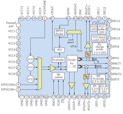
A pair of integrated circuits (ICs) from Analog Devices provides a solution by redefining the meaning of “mixer” in receiver front ends. Essentially, the ICs incorporate many of the components once added to a mixer in a receiver—such as local oscillators (LOs) and intermediate-frequency (IF) amplifiers—within the mixer IC itself. They make it possible to dramatically shrink a cellular base station while also providing software-defined-radio (SDR) flexibility to handle a number of different wireless standards.
The ICs in question are the models ADRF6612 and ADRF6614, both designed for RF ranges of 700 to 3,000 MHz, LO ranges of 200 to 2,700 MHz, and IF spans of 40 to 500 MHz. They work with low- or high-side LO injection and include an on-board phase-locked loop (PLL) and multiple low-noise voltage-controlled oscillators (VCOs), all packed within a 7- × 7-mm, 48-lead LFCSP housing. This level of integration and component density is enhanced by the diversity and programmability to support a number of different wireless standards in the small volumes required by modern microcells.
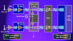
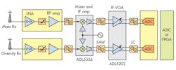
To appreciate the savings in space offered by these highly integrated mixer ICs, it may help to remember the front end of a cellular base-station receiver from around 2010 (Fig. 1). The dual-mixer architecture covered a bandwidth of approximately 1 GHz, requiring multiple components to handle the then cellular frequency range of 800 to 1,900 MHz. Frequency synthesis was provided by a separate PLL and narrowband VCO module that required a unique PLL loop filter for optimum performance. Dedicated VCO modules were used for each band of interest, adding to the required circuit-board area within the base station.
In addition, these discrete components were interconnected by low-impedance transmission lines, which contributed some signal loss. As a result, generous current was needed to drive the VCO output to a sufficient level for the mixer for low phase noise and noise figure under signal-blocking conditions.
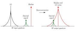
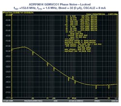
Receiver ICs with integrated VCOs are not new. But achieving the wide bandwidths and low phase-noise levels required by multiple-carrier Global System for Mobile Communications (MC-GSM) wireless networks has been a challenge. The channel reuse scheme of GSM requires that receive LOs have extremely low phase noise, particularly at an alternate-channel offset frequency of 800 kHz (Fig. 2). If excessive phase noise at these alternate channels mixes with unwanted signals at the same 800-kHz offset, it can result in phase noise translated to the IF output, degrading system sensitivity.
Low VCO phase noise is typically achieved with a high-quality-factor (high-Q) tank and narrowband design. Frequency division can also reduce noise. By operating a VCO at an integer multiple of a receiver’s LO frequency, a 6-dB/octave reduction in phase noise is achieved by the subsequent division (Fig. 3). The phase-noise requirements for GSM in the 1,800- to 1,900-MHz band are extremely difficult—roughly twice as severe as those in the 800- to 900-MHz band.
In addition to low phase noise, modern base-station receiver designs must support the many modulation schemes currently used in wireless communications networks. In addition to GSM, other modulation schemes include wideband code-division-multiple-access (WCDMA) and Long Term Evolution (LTE) systems. Receiver designs often consist of a number of different VCOs with moderate phase-noise performance levels configured so that they are combined to cover an octave bandwidth within the base station.
Once a number of VCOs have been configured to generate an octave bandwidth for the highest frequencies of operation, lower LO frequencies can be achieved by binary division. This approach was used in the ADRF6612 receiver mixer, where VCO fundamental frequencies span 2.7 to 5.6 GHz and two stages of frequency division realize LO frequencies from 200 to 2,700 MHz by dividing from 1 to 32. For applications that also include MC-GSM, the ADRF6614 receiver mixer includes two additional high-performance VCO cores to provide the LO frequencies needed for the 1,800- to 1,900-MHz GSM bands.
Since modern wireless microcells may not have the benefits of climate-controlled environments, components such as these receiver ICs must provide consistent, reliable performance over wide temperature extremes. To achieve specified performance over a wide operating temperature range, the PLLs and VCOs in the ADRF6612 and ADRF6614 ICs employ a number of calibration techniques.
For wide bandwidths with low noise, each VCO core employs an 8-b capacitive digital-to-analog converter (CDAC) that automatically selects the correct band (1 of 128) for a given LO frequency. Any variations in VCO tank amplitude are carefully monitored by the system, and the amplitude is adjusted using an automatic-level-control (ALC) system for optimum output amplitude. Each IC performs a calibration sequence any time the operating frequency is reprogrammed. This ensures that the selected band centers the tuning voltage for a VCO’s tuning varactor diode in the optimum range to maintain the synthesizer in lock over the required operating temperature range.
The four VCO cores in each ADRF6612 and ADRF6614 ICs are positioned to ensure that their operating ranges provide suitable overlap for changing environmental conditions and device fabrication tolerances. The cores will generally move frequency in the same direction for environmental and process variations, so there is enough overlap built in for the frequency synthesizer to always achieve locked conditions.
Once the calibration solution is determined, frequency should be maintained indefinitely; the tuning voltage range supports the required hold-in range. In time-division-duplex (TDD) systems, where the base station may change frequencies on a time-slot-to-time-slot basis, this operating time may be measured in microseconds. In frequency-division-duplex (FDD) systems, it might be necessary to maintain lock on a single frequency for years.
There is no allowable downtime at any point during the system operation of the ADRF6612 and ADRF6614 ICs. Thus, changes in temperature and component aging effects are covered by the varactor tuning-voltage range and frequency tuning sensitivity (Kv) of the VCO for potentially a 145°C temperature range. Each IC constantly monitors device temperature and adjusts the VCO bias as required.
The ADRF6612 and ADRF6614 ICs use a unique approach to minimize degradation of receiver sensitivity from spurious signal products. Using the synthesizer’s integer mode with a tight loop filter results in low reference spurious products of less than −100 dBc. Minimal spurious signals are critical for modulation schemes such as MC-GSM. For LTE and other modulation schemes, or where fine frequency steps are required, the synthesizer can be operated in fractional-N division mode. The reference path incorporates a 13-b divider, and the integer and fractional paths each incorporate 16-b dividers for flexibility.
For applications where co-located, phase-tracked receive channels are required, such as in multiple-input, multiple-output (MIMO) systems, multiple ADRF6612 and ADRF6614 ICs can be cascaded in a daisy-chain manner to permit one unit acting as a master synthesizer to supply additional slave receivers through their external LO output and input ports, respectively. In this way, additional LO distribution amplifiers and their associated increases in phase noise can be minimized.
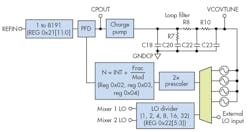
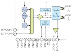
To support both high- and low-side LO injection, each IC’s LO chain provides flexible signal processing (Fig. 4). Using integer division ratios of 1 to 32, low-side injection is possible even for the 700-MHz band with a high IF. The LO stages also provide a square-wave drive to the passive mixer cores over the full LO range from 200 to 2,700 MHz.1
Modern wireless base-station receivers must operate in typically hostile signal environments. For example, any other in-band signals close in frequency to low-level input signals to the cellular receiver can act as blocking signals. In such a case, phase noise from the LO amplifier in the vicinity of the blocking signal is mixed into the IF output band directly on top of the desired signal. This increases the noise floor and reduces the signal-to-noise ratio (SNR) of the receiver—sometimes dramatically.
Since the blocking signal may be large (high power), it is important that both the VCO phase noise be extremely low, and the LO chain does not degrade the noise floor at the blocker offset. At these very high blocking levels, the receiver noise figure will eventually become dominated by the blocking signal and degrade according to the power level of the blocker.
In discrete implementations of the receive chain, it would be possible to introduce some filtering into the LO path to minimize the phase noise at the blocker offset coming from the VCO and LO distribution amplifiers. However, in an integrated front end, care must be taken to avoid additive phase noise in the LO chain.
The ADRF6612 and ADRF6614 ICs employ a high-gain LO chain and hard-limiting amplifiers to drive the LO chain into limiting. As each stage enters hard limiting, the small-signal gain of the LO chain that would otherwise increase phase noise is substantially reduced, minimizing noise-figure degradation under blocking conditions.
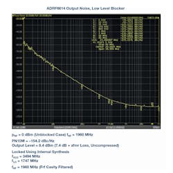
The noise fold-over from the blocking signal degrades the output noise spectrum of the receiver, and hence the receiver noise figure, by raising the output noise floor. The ADRF6612 and ADRF6614 receiver ICs are designed to withstand significant blocking signals with minimal degradation of receiver noise figure (Fig. 5). Even with a +10-dBm input blocking level, the receiver’s noise figure is only degraded by 3.2 dB at 10 MHz offset from the carrier, even though the conversion gain is compressed by 1 dB at that extreme blocking level.
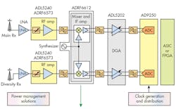
The high level of integration in these receiver ICs has enabled significant performance improvements and savings in dc power for modern wireless base-station designers (Fig. 6). The ICs feature a technique that simultaneously optimizes the RF and IF stages surrounding the on-chip mixer.2
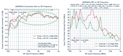
This technique, first implemented in the ADRF6612, provides a minimum IIP3 of over +25 dBm over temperature and the full frequency range with low power dissipation, and +29 dBm up to 2 GHz over temperature. The technique also provides optimum receive path noise-figure performance with high conversion gain (Fig. 7).3,4
Acknowledgments
With the increased level of integration inherent in complete receiver chains comes a much larger development team. While it isn’t possible to list all of the people that contributed to this work, the authors take great pleasure in acknowledging the efforts of the following industry experts: Kurt Fletcher and Dominic Mai spent many hours implementing an excellent layout while maintaining symmetry and avoiding unwanted couplings. Vincent Bu worked to develop the necessary packaging with our vendors. Susan Stevens maintained the excellent working relationship with our external foundry partner. Craig Levy and Rachana Kaza developed the production test capability for these parts. Wendy Dutile, Ed Gorzynski, and Chris Norcross all participated in the extensive prototyping of the test circuitry. Mark Hyslip coordinated the business aspects of successfully bringing this project together. The authors would like to dedicate this work in the memory of our colleague, Edward J. Gorzynski.
Marc Goldfarb, Design Engineer
Ben Walker, Design Engineer
Russell Martin, Product Engineer
Tom Bosia, Product Engineer
Ed Balboni, Design Engineering Manager
Dragoslav Culum, Marketing Engineer
Analog Devices Inc., 804 Woburn St., Wilmington, MA 01887; (781) 329-4700
References
1. M. Goldfarb, R. Martin, and E. Balboni, “Novel Topology Supports Wideband Passive Mixers,” Microwaves & RF, October 2011, pp. 90.
2. “Apparatus and Method for a Wideband RF Mixer,” US Patent 8,571,511 (A Technique for Optimizing the Performance of a Wideband Passive RF Mixer through the Employment of a Unique Multi-frequency Tuning Topology).
3. ADRF6612 datasheet, Analog Devices Inc. © 2014-2016.
4. ADRF6614 datasheet, Analog Devices Inc. © 2016.
