This file type includes high resolution graphics and schematics when applicable.
Designers of battery-powered, portable communications devices continue to aim for lower-power operation even as the complexity of these devices increases. One excellent illustration of this trend is Linear Technology’s model LTC5599 direct-conversion in-phase/quadrature (I/Q) modulator, which provides excellent performance from 30 MHz to 1.3 GHz, in spite of requiring a mere 28 mA current from a supply of +2.7 to +3.6 VDC. Housed in a 24-lead, 4-×-4 mm QFN package, the I/Q modulator is extremely compact and is suitable for low-power use in a wide range of applications, including wireless microphones; commercial and military software-defined radios (SDRs); battery-powered military and commercial radios, satellite-communications (satcom) systems; and wireless networks.
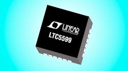
The model LTC5599 I/Q modulator (Fig. 1) is designed for direct modulation of differential I and Q signals onto an RF carrier signal. By applying 90-deg. phase-shifted signals to theI and Q signals, single-sideband (SSB) or sideband- and carrier-suppressed upconversion can be achieved. As a simple block diagram of the modulator shows (Fig. 2), it is essentially a pair of RF mixers and a power combiner, but includes control of I and Q baseband input channels and a serial peripheral interface (SPI) bus. The modulator consumes very little energy from low-voltage sources and can be used with sine-wave or square-wave local oscillator (LO) drive.
The SPI bus provides control of modulator gain, and can optimize LO carrier feedthrough and sideband suppression. The modulator integrated circuit (IC) even includes a thermometer that can be activated to compensate for gain variations with temperature to maintain stable modulation levels across wide operating-temperature ranges (the LTC5599 is specified for case operating temperatures from -40 to +105°C). The packaged modulator also provides a continuous analog gain-control pin (VCTRL) for high-speed control of power levels.
In terms of performance, the LTC5599 modulator provides reliable control of desired signals and helps minimize undesired signals. The SPI bus, for example, allows control of I/Q gain from -19 to 0 dB in 1-dB steps (with the gain level impacting the current consumption). LO carrier leakage of only -65 dBm; LO carrier leakage is typically just -51.5 dBm at 500 MHz, but can be lowered to -65 dBc with the I and Q offset adjustment. The sideband suppression is typically -52.6 dBc at 500 MHz, which can similarly be reduced by means of I/Q gain and phase adjustment to a mere -60 dBc.
The LTC5599 I/Q modulator provides healthy output third-order-intercept-point (IP3) of +20.8 dBm at 500 MHz. It features low RF output noise floor of -156 dBm/Hz at 6 MHz offset from the carrier, when measured with an RF output power level of +3 dBm. The modulator’s excellent image rejection and carrier suppression help improve wireless transmitter performance while the low-power operation can help extend battery operating time. With the SPI bus and the modulator’s adjustable gain, it can also help to minimize the need for additional external components, contributing to lower costs in some of these battery-powered applications.
Linear Technology Corp., 1630 McCarthy Blvd., Milpitas, CA 95035-7417; (408) 432-1900, FAX: (408) 434-0507.
This file type includes high resolution graphics and schematics when applicable.


