Picking PCB Materials for Microwave Amps
This file type includes high resolution graphics and schematics when applicable.
Microwave amplifiers come in many shapes and sizes, with low-noise amplifiers (LNAs) and power amplifiers (PAs) perhaps two of the most commonly used high-frequency varieties. One of the most essential components in implementing both types of amplifiers in hybrid circuit form is the printed-circuit board (PCB) which can contribute a great deal to the final performance of both LNAs and PAs, of course in different ways.
By reviewing some basic PCB material characteristics and parameters, it can be possible to locate available PCBs that are well suited to LNA and PA circuit designs for a wide range of commercial, industrial, and military applications.
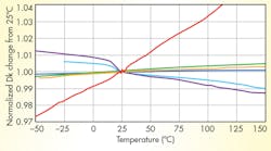
Consistency and stability are two properties that might be considered good starting points for any circuit material being considered as a foundation for either an LNA or a PA (Fig. 1). The power levels and the heat generated by the two types of amplifiers will differ, but maintaining consistent behavior across frequency and temperature for critical PCB material parameters—such as dielectric constant (Dk or εr), temperature coefficient of dielectric constant (TCDk), or dissipation factor (Df)—can benefit the performance of either type of amplifier.
LNAs are typically compared for a given bandwidth by a number of key performance parameters, including noise figure, small-signal gain, and output power at 1-dB compression. Ideally, noise figure remains consistently low even with increasing frequency and temperature. LNA noise figure is highly dependent on tight impedance control of the LNA circuitry (often at 50 Ω), and tight impedance depends on a number of different circuit material characteristics. These include variations in PCB material thickness, variations in Dk across the material, and changes in Dk as a function of temperature.
Minimizing circuit material loss will contribute to minimizing the noise figure of an LNA fabricated on that material.1 PCBs suffer losses from various components of the material, including dielectric loss from the dielectric material. For that reason, PCBs with lower Df values are usually specified for RF/microwave LNA designs.
Variations in material thickness can produce variations in the impedance of transmission lines fabricated on those circuit materials, so a candidate PCB material for an LNA design should have tightly controlled thickness to enable tight impedance control for those PCBs. Materials with thickness tolerances of ±10% or better are considered quite good for many high-frequency applications.
For a PCB with a given Dk value, the circuit characteristic impedance is determined by the width of the transmission-line conductors and the Dk value. For lower-Dk materials, wider conductors are needed to achieve a given impedance (such as 50 Ω) compared to narrower conductors for the same impedance with higher-Dk materials. Although these wider transmission lines may occupy more space on the PCB, they also suffer lower loss than narrower transmission lines.
Of course, a circuit material’s Df also contributes to the material’s loss calculations. Achieving tight impedance control for a particular PCB material requires minimizing variations in PCB conductor width and minimizing the variations in the thickness of the copper used to form those conductors. The impact of conductor and copper thickness variations on impedance is greater for thinner PCB materials than for thicker PCB materials, although those thicker PCB materials will have greater dielectric losses than the thinner circuit materials.
Circuit impedance also varies with changes in circuit Dk, so a candidate PCB material for an LNA should offer fairly tight Dk tolerance. Fortunately, commercial PCB materials are available with Dk values held within fairly tight tolerances across the material. For example, RT/duroid 6035HTC material from Rogers Corp. exhibits a Dk of 3.5 through the z-axis (thickness) of the material at 10 GHz, with a Dk tolerance within ±0.05 across the material. The tightly controlled Dk makes possible LNA circuits with tightly controlled impedance for strong noise-figure performance.
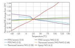
The RT/duroid 6035HTC material maintains tight Dk across a wide temperature range (Fig. 2), with a TCDk of -66 ppm/°C in the z-axis from -50 to +150°C. The material also exhibits low loss, with a Df of 0.0013 at 10 GHz. This material and these characteristics are good examples of the types of material specifications that can combine for good LNA performance.
This file type includes high resolution graphics and schematics when applicable.
PA Materials
This file type includes high resolution graphics and schematics when applicable.
Circuit materials for RF/microwave PAs have a somewhat different set of priorities for their critical characteristics since they are processing much higher power levels than LNAs.2 As with circuit materials for LNAs, tight Dk and impedance control are important parameters for materials being considered for PA circuits. Thermal conductivity becomes a bit more important for PA designs owing to the greater heat generated by these types of amplifiers. In fact, key PCB material parameters to consider for PAs are thermally related, including thermal conductivity, TCDk, and coefficient of thermal expansion (CTE).
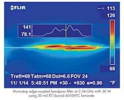
High-frequency circuit materials are often referred to as thermally resistive materials since they typically offer low thermal conductivity. A typical minimum value of thermal conductivity for a circuit material for a PA is about 0.30 W/m/K. But commercial PCB materials are being developed with increasing values of thermal conductivity in support of PA circuit designers.3 Ideally, PCB materials for PAs can exceed that 0.30 W/m/K value of thermal conductivity, to aid in the thermal management of the active devices, such as gallium-nitride (GaN) transistors, that amplify high-frequency signals and generate heat in solid-state RF/microwave PAs. The RT/duroid 6035HTC circuit material referenced earlier actually has a remarkably high thermal conductivity compared to most commercial circuit materials—1.44 W/m-K at +80°C—which makes this material a strong candidate for RF/microwave PA circuits especially at higher power levels where more heat must be removed from the PCB.
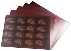
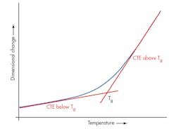
The same material’s TCDk characteristics indicate that, as it does for LNAs, it will maintain consistent Dk behavior for PAs across a wide operating temperature range (Fig. 3). In addition, with CTE that is closely matched in the x and y axes (19 ppm/°C) to the CTE of the copper (17 ppm/°C) that forms the conductors for the circuit material, RT/duroid 6035HTC material (Fig. 4) promises to provide reliable plated through holes (PTHs).
This holds true even with the thermal stress that can be exerted by some high-frequency PA circuits. Such PTHs may be needed for conducting heat from active devices and PA circuitry, through the PCB dielectric material, and to a metal base plate where the heat can be dissipated as part of a thermal-management arrangement.
PCB material loss plays a role in the amount of gain and output power that can be achieved for a given PA circuit, with circuit material loss varying with material thickness. Circuit materials have numerous loss components, such as conductor and dielectric losses, that vary in their percentage of the total PCB loss as a function of material thickness.
For example, with thicker PCB materials, dielectric losses comprise a larger portion of the total loss, whereas with thinner PCB materials, conductor losses are more dominant. Selecting PCB materials with lower total losses can help to optimize PA performance in terms of both gain and output power.
A PCB material’s copper surface roughness can play a role in the material’s conductor-loss performance. A material with rough copper surface will have increased conductor loss compared to the same circuit material with smooth copper surface. Again, it will have greater effect on the total PCB loss for thinner circuits rather than for thicker circuits, where dielectric losses are more dominant.
Building PAs on PCB materials with high loss not only can rob the design of output power and gain, but also contribute to thermal-management challenges, since the higher loss means that more power through the amplifier is translated into heat. One material parameter that serves as a reliable guideline for the thermal management of a PCB PA design is the PCB’s maximum-operating-temperature (MOT) specification, which should not be exceeded for any length of time if at all possible.
The heat generated by a PA design can be decreased by selecting a PCB material with thickness and loss that are optimum for the PA’s expected output-power levels. Otherwise, thermal-management steps must be taken, such as the addition of heat sinks to the PCB, to ensure that the PCB MOT is not exceeded for that PA design.
This file type includes high resolution graphics and schematics when applicable.
Higher Dk Materials
This file type includes high resolution graphics and schematics when applicable.
In the search for PCB materials for LNAs and PAs, circuit materials with higher Dk values offer the opportunity to miniaturize circuit dimensions for a given impedance and frequency range when physical size is critical.4 The wavelength of a circuit is frequency dependent and material dependent, and PCB materials with higher Dk values result in circuit structures operating at shorter wavelengths for a given frequency.
For various circuit elements that are wavelength dependent, such as antennas and filters, the use of higher-Dk circuit materials can result in smaller PCBs. Commercial PCB materials for RF/microwave applications are typically in the Dk range of 2 to 6, so “high-Dk” circuit materials are generally considered to be those materials with Dk of 6 or higher.
As an example, RO4360G2 circuit material from Rogers Corp. has a Dk of 6.15 in the z-axis at 10 GHz (with a tight Dk tolerance of ±0.15) with thermal conductivity of 0.75 W/m/K and low Df of 0.0038. The higher Dk of the material enables smaller dimensions for wavelength-dependent structures. The material is often combined with lower-Dk circuit materials in multilayer circuit designs and it can be processed with the same approaches as used for lower-cost circuit materials, such as FR-4.
For an even higher Dk value, RO3210 circuit material from Rogers Corp. has Dk of 10.2 in the z-axis at 10 GHz, held to a tolerance of ±0.50. It has very low loss, with Df of 0.0027, and slightly higher thermal conductivity than the RO4360G2 material, at 0.81 W/m/K. The very high Dk value of this material enables dramatic reductions in wavelength-dependent circuit structures when circuit miniaturization is an issue.
In short, when designing an RF/microwave amplifier—whether an LNA or a PA—the quest for a suitable PCB material involves reviewing many of the same material parameters, with consistent Dk critical for maintaining the stable impedance needed for both types of amplifiers. Circuit materials capable of maintaining Dk within a tight tolerance window over wide temperature ranges can help achieve the low noise figure and flat gain desirable for high-frequency LNA designs.
In the case of PA designs, materials with tight Dk and consistent thermal properties (including TCDk and CTE) and low loss (low Df) can serve as excellent starting points for high-power amplifiers that can effectively dissipate generated heat.
John Coonrod, Technical Marketing Manager
Rogers Corp., Advanced Connectivity Solutions, 100 South Roosevelt Ave., Chandler, AZ 85226-3416; (480) 961-1382
References
1. John Coonrod, “Picking Proper PCB Materials For LNAs,” Microwaves & RF, July 2014, pp. 69-72.
2. John Coonrod, “Packing Power Into Microwave PCBs,” ROG Blog #82, Rogers Corp.
3. Jack Browne, Circuit Laminate Keeps The Heat Out,” Microwaves & RF, April 2011, p. 105.
4. John Coonrod, “Benefit from High-Dk Microwave Circuit Materials,” Microwaves & RF, October 2013, pp. 62-70.
This file type includes high resolution graphics and schematics when applicable.
