Balanced Amplifier Aims For Low Noise
This file type includes high resolution graphics and schematics when applicable.
Minimizing noise has been an ongoing challenge for architects of communications systems, especially for designers of low-noise amplifiers (LNAs). A balanced LNA configuration can provide many advantages compared to single-ended amplifiers in terms of very low mismatch and stability, albeit with slightly higher current requirements. For high performance at 1.9 GHz, a balanced LNA was developed based on a new dual-amplifier GaAs high-electronic-mobility-transistor (HEMT) monolithic microwave integrated circuit (MMIC). It features low noise figure and high gain, and is based on readily available commercial circuit components and printed-circuit-board (PCB) materials.
A key to achieving low noise figure in a balanced amplifier is the choice of quadrature 3-dB couplers (also known as 90-deg. or hybrid couplers) used to join the constituent amplifiers.1,2 A balanced amplifier configuration can also provide improved reliability, linearity, and bandwidth compared to a single-ended amplifier,3 albeit while requiring twice the current and circuit components of the single-ended amplifier.
Of course, in a balanced amplifier, the quadrature couplers represent additional cost, occupy substantial PCB space, and exhibit insertion losses that degrade amplifier noise figure, gain, and output power. For applications like tower-mounted amplifiers (TMAs), LNAs should ideally be as small and light in weight as possible. Shrinking the couplers can be critical to reducing the balanced LNA size.4-9 Integrating multiple functions at the module11,12 or chip13-15 levels can also minimize the size of an LNA for use as a TMA. But efforts at LNA miniaturization are usually limited by the levels of performance expected from the amplifier, since a small size usually means limited performance.
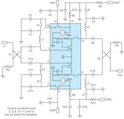
1. This block diagram shows the on- and off-chip components for the balanced LNA, where the components labelled JU are 0-Ω chip resistors that bridge breaks in the copper traces (but not essential to the design).
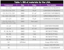
A high-performance 1.9-GHz balanced LNA was achieved by integrating dual amplifiers and other key functions on a new MMIC chip and using that as the basis for the LNA (Table 1). To minimize component count, dual amplifiers, electrostatic discharge (ESD) protection, active bias, and shutdown functions were integrated on MMIC (the yellow area in Fig. 1). Combining bias circuitry and amplifiers on the same chip helps stabilize the operating current against variations in gate threshold voltage and temperature. MMIC chips were fabricated on 6-in. GaAs wafers using a proprietary 0.25-μm enhancement-mode pseudomorphic high electron mobility transistor (ePHEMT) process. The same process had already been used to fabricate a single-ended LNA with 0.5-dB noise figure at 1.9 GHz.6 It was thus thought to be possible to provide a balanced amplifier with 0.7-dB noise figure and target gain of better than 17.6 dB at 1.9 GHz, after considering the coupler’s loss.
The ePHEMT process features a relatively high transition frequency (fT) of better than 30 GHz and peak transconductance of about 615 mS/mm, with stable linearity down to +2 VDC.7 This is essential for a cascade amplifier arrangement where each transistor only receives one-half of the power supply. The MMIC chips were placed on a copper lead-frame, connected to the amplifier leads with bond wires, and then epoxy molded to form a 16-pin, 4 x 4 x 0.85 mm quad flat no-lead (QFN) package.
Because a single common-source ePHEMT stage falls about 1.6 dB short of the 17.6-dB LNA gain target at 1.9 GHz,11 a two-stage cascade or cascode configuration was needed for higher gain. The cascode approach was selected for its excellent power consumption. The cascode amplifier’s upper gate is biased by an internal resistor divider, while inductor L1/L2 connects the lower gate to adjustable active bias. External inductors were used rather than on-chip components because of their low losses and for the flexibility of tuning if necessary. Wire-wound chip inductors rather than multilayer inductors were used to achieve low noise figure. Along with their bias functions, the inductors and series capacitors C3 and C16 also form highpass filtering functions to roll off unneeded low-frequency gain from the active devices.
The balanced LNA circuit includes a shutdown function block consisting of a transistor switch in series with the active bias circuitry. Shutdown is initiated by applying a high-logic (≥ 2) signal at port Vsd1/2 to open the switch. Conversely, a low-logic signal (i.e., Vsd1/2 ≤ 500 mV) enables the amplifiers. Transitioning from normal to shutdown mode takes less than 32 ns if the large (≥ 0.1 μF) decoupling capacitors (C8, C22, C23, and C24) are omitted. However, these capacitors are generally recommended to ensure low-frequency stability and supply transient dampening.
The balanced amplifier’s signal splitting and combining utilize commercially available multilayer quadrature hybrid couplers, denoted X1 and X2, to save design effort and PCB space. To minimize input loss, a larger (6.4 x 5.1 mm) coupler, X1, is used at the input, while a smaller (2.0 x 1.3 mm) coupler, X2, is used at the output to save space and cost. To ensure that volume production can consistently achieve input return loss of better than 21 dB, Monte Carlo analysis was used to identify critical parameters. Two controls were instituted for a dual purpose: correlating the amplifiers’ input match to |S11a – S11b| < 0.025, and ensuring that the input coupler delivers more than 26-dB isolation. The first control is satisfied by assembling with adjacent chip while the second control requires tightening the coupler isolation above the guaranteed 23 dB.8 The output coupler is not critical in achieving these goals.
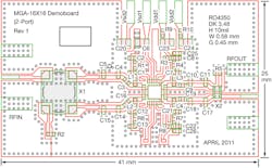
2. This PCB layout shows the placement of components in the balanced LNA, all within a 30 x 15 mm area.
The LNA’s PCB (Fig. 2) is based on 10-mil-thick RO4350B laminate from Rogers Corp. Microstrip transmission lines were dimensioned for 50-Ω characteristic impedance whenever practical. The transmission lines next to the input coupler’s mounting pads were scaled down following the coupler manufacturer’s recommendations to compensate for the parasitic capacitances of the coupler pads. An FR-4 layer was added to the RO4350B to increase the stack height to 1.6 mm. Input and output microstrip lines were transitioned to coaxial connectors using edge-launched SMA receptacles, with all amplifier performance results referenced to the coaxial terminations.
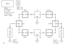
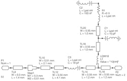
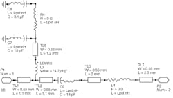
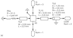
The LNA circuit model was split into a two-level hierarchy (Fig. 3) suitable for simulation with the ADS2009 computer-aided-engineering (CAE) software from Agilent Technologies. The upper level consists of blocks representing the MMIC, the signal dividing/combining,and the impedance matching functions. Each of the dual amplifier stages, Q1 and Q2, is represented by an identical set of two-port S-parameter (.s2p) files. The amplifier’s .s2p files were previously extracted on a test fixture based on similar 10-mil RO4350B PCB material, with through-reflect-line (TRL) calibration performed on a commercial vector network analyzer (VNA) to shift the reference planes of the amplifier to the package edges.
3. These equivalent-circuit models represent the top-level circuit model, subcircuits of the input combining section and input matching network, and the output combining and matching subcircuits.
The device’s noise and linearity (third-order intercept point; IP3) parameters were extracted using commercial source- and load-pull impedance tuners with the same test fixture. A minimum noise figure (NFMIN) of 0.3 dB is difficult to extract because it can be easily obscured by the combined losses of the mechanical impedance tuner and the APC7-to-3.5-mm connector adapter. The inductors and hybrid couplers were modelled by means of their manufacturers’ .s2p data. Other passive components were modelled using their equivalent-circuit models and lower-order parasitic elements.
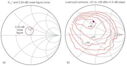
To validate the input and output matches, the modelled source (ΓS) and load (ΓL) impedances were compared with the aforementioned source- and load-pull contours (Fig. 4). Both ΓS and ΓL were simulated with the aid of the S-parameter probe component in the ADS software. The results confirm that the matching networks are close to optimum.
4. The ΓS and ΓL positions on the noise contours (left) and on the output IP3 contours (right) validate that the accuracy of the matching networks.
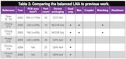
Among TMA-capable balanced LNAs, this new LNA design sets new milestones in size reduction and function integration (Table 2). It is 40 to 110% smaller than those earlier designs. The parts count is higher than multichip-on-board (MCOB) designs with integrated impedance matching,11,12 but the new LNA’s external matching enables lower noise figure; its monolithic fabrication is also lower in cost than those other designs. The dual-amplifier MMIC also integrates as many functions as the best of the prior arts, and appears to be the first dual-amplifier MMIC that integrates the shutdown function.
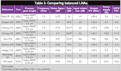
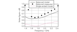
Miniaturization need not detract from noise performance; in fact, the new design’s noise figure is second only to a competing design using a shorter-gate-length device14 as noted in Table 3. The LNA’s experimental noise figure is 0.65 dB at 1.9 GHz, or within 0.1 dB of the prediction (Fig. 5). The simulation model’s errors increase towards the band edges. Both predicted and experimental (measured) noise figure minima are offset to 1.7 GHz, but retuning is not necessary since the potential improvement will only be about 0.05 dB. Since the device-level noise figure of a single-ended amplifier is about 0.3 dB, a noise figure of 0.3 dB is inferred for the combined loss of the coaxial connector, coupler, and input impedance matching network. The noise figure is only marginally worse (about 0.01 dB) than a previous design that used a 55% larger coupler,13 even though the two couplers’ maximum loss specification differs by 0.1 dB (0.22 dB vs. 0.12 dB).
5. The modelled and measured noise figures for the balanced LNA agree closely. The single-ended amplifier noise figure is also shown as a reference since its difference from the noise figure of the balanced amplifier allows the input coupler’s loss to be estimated.
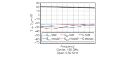
In spite of the efforts to achieve a miniature design, the LNA achieves best-in-class return-loss and gain performance levels. The gain is 19 dB at 1.9 GHz, with 32-dB input return loss and 27-dB output return loss (Fig. 6), and good agreement between simulated and measured results. The best input return loss is at 1.9 GHz because it coincides with the center frequency of the input coupler. Similarly, the best output return loss is at 1.75 GHz, and this is also a property of the coupler. Although the circuit model is less accurate for return loss than for gain, the mismatch is minimal—at less than 22 dB across a 500-MHz span. The LNA’s bandwidth exceeds 500 MHz at the 20-dB return-loss points. The best achievable return loss is limited by the couplers’ finite isolation and by the microstrip discontinuities.
6. These plots show the modelled and measured gain and return loss for a center frequency of 1.9 GHz.
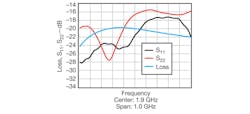
When the MMIC’s shutdown function is activated, the amplifier is transformed into a nonreflective attenuator, which can be used to prevent overloading. In this state, it provides 20-dB attenuation at 1.9 GHz, with input and output return losses of 22.0 and 16.5 dB, respectively (Fig. 7). It achieves good match during shutdown mode since reflected energies are cancelled in the couplers. In contrast, an unpowered single-ended amplifier will be highly reflective, requiring that it be bypassed to prevent detuning of any connected antenna and filter.
7. The excellent return loss (better than 16 dB) during the balanced LNA’s shutdown mode may eliminate the need for bypassing the amplifier.
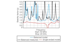
The balanced LNA is unconditionally stable even when its constituent amplifiers are not. The stability factor, μ, exceeds unity from 50 MHz to 20 GHz (Fig. 8) when modelled or measured. The balanced topology proves to be self-stabilizing even when modeled with unstable (μ < 1) individual amplifiers from 6 to 18 GHz. The model is generally accurate below 8 GHz but, above this limit, the accuracy suffers from gross oversimplification of the passive components’ equivalent circuits.
8. The balanced LNA features simulated and measured stability factor, μ, of better than unity across a wide frequency range.
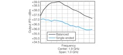
The LNA’s linearity is superior to other amplifiers that consume about the same power, about 0.5 W. The output third-order-intercept point (OIP3) is +38.9 dBm at 1.9 GHz (Fig. 9), peaking at 1.75 GHz, the minimum output-return-loss point. The OIP3 improvement over the constituent amplifiers is about 0.7 dB lower than predicted by theory due to the loss of the output coupler. The linearity figure of merit calculated from the ratio of the OIP3 to the DC power is 7.943/0.51 or approximately 15.6.
9. The output third-order-intercept performance for the balanced amplifier is considerably higher than for a single-stage amplifier across the same frequency range.
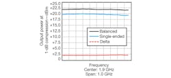
The balanced amplifier provides +22.4-dBm output power at 1-dB compression (P1dB) at 1.9 GHz. This is about 0.6 dB lower than a single-stage design theoretically due to the output coupler’s loss (Fig. 10). High P1dB provides better immunity to changes in gain and noise figure because of a strong interferer/blocker. The amplifier also has a 16.9-dB difference between P1dB and OIP3, considerably higher than values achieved by the other LNA approaches.
10. Output power at 1-dB compression remains flat across a 1-GHz bandwidth centered at 1.9 GHz.
This miniature balanced LNA design provides state-of-the-art results for low reflection, low noise-figure, and outstanding linearity performance. Its excellent impedance matching in shutdown mode can potentially eliminate the need for bypassing the LNA. The dual-amplifier MMIC is well suited to alternative wireless applications, such as balun-less connections to balanced antennas.18,19
Chin-Leong Lim, Engineer
Avago Technologies, 11900 Bayan Lepas, Penang, Malaysia; (604) 610-2525, www.avagotech.com.
Acknowledgments
The author thanks Zulfa for the device design, M.D. Suhaiza and S. Punithevati for the prototype assembly, S.A. Asrul for reviewing the draft, and the management of Avago Technologies for approving the publication of this work. Special thanks is also due to Anaren Communications (Suzhou), which provided the couplers at no charge.
References
1. M. Eisele, R.S. Engelbrecht, and K. Kurokawa, “Balanced Transistor Amplifiers for Precise Wideband Microwave Applications,” IEEE International Solid-State Circuits Conference, February 1965.
2. R.S. Engelbrecht and K. Kurokawa, “A Wideband Low Noise L-Band Balanced Transistor Amplifier,” Proceedings of the IEEE, Vol. 53, No. 3, March 1965, pp. 237-247.
3. Steve Cripps, RF power amplifiers for Wireless Communications, Artech House, Norwood, MA, 1999, Section. 10.2 “Balanced amplifiers.”
4. J.S. Mandeep and H. Abdullah, “A compact, balanced low noise amplifier for WIMAX base station applications,” Microwave Journal, November 2010.
5. A.F. Osman and N. Mohd. Noh, “A design for SDR radio using balanced amplifier topology,” 4th Asia Symposium on Quality Electronic Design, 2012.
6. Avago Technologies, Application Note 5475, “MGA-634P8 GaAs ePHEMT MMIC,” www.avagotech.com.
7. J. Madden, “Low voltage operation of GaAs power amplifier,” Microwave Journal, September 2006, pp. 130-134.
8. Anaren Microwave, Product Specification “X3C19P1-03S hybrid coupler,” Rev. D, www. anaren.com.
9. Avago Technologies, Application Note 1281, “A High IIP3 Balanced Low Noise Amplifier for Cellular Base Station Applications Using the Enhancement Mode PHEMT ATF-54143 Transistor and Anaren Pico Xinger 3 dB Hybrid Couplers,” www.avagotech.com.
10. I. Piper, S. Seward, A. Ward, H. P. Hostergaard, and S. Tozin, “Balanced LNA suits cellular base stations,” Microwave & RF, April 2002, pp. 70-80.
11. T. Chong, “A Low-Noise, High-Linearity Balanced Amplifier in Enhancement-mode GaAs pHEMT Technology for Wireless Base-Stations,” Proceedings of the European Microwave Conference, Paris, France, October 2005.
12. T. Chong and S. Rendava, “Design and Performance of a 1.6-2.2-GHz Low-Noise, High Gain Dual Amplifier in GaAs E-pHEMT,” Asia Pacific Microwave Conference, Suzhou, China, December 2005.
13. Avago Technologies, Application Note 5442, “LNA Design with the MGA-17516 Matched Pair, Low Noise Amplifier,” www.avagotech.com.
14. Ommic product specification, “CGY2105XHV Dual Ultra Low Noise High IP3 Amplifier,” www.ommic.com.
15. Ommic product specification, “CGY2106XHV Dual Ultra Low Noise High IP3 Amplifier,” www.ommic.com.
16. B. Jensen, “Build LNAs with an integrated approach,” Microwaves & RF, December 2002.
17. X.Y. Gao, W.K. Xie, and L. Tang, “Optimum design for a low noise amplifier in S-band,” Journal of Electronic Science and Technology of China, Vol.5, No.3, pp. 234-237, September 2007.
18. J. Morawietz, R.H. Witvers, J.G.B. de Vaate, and E.E.M. Woestenburg, “Noise characterization of ultra low noise differential amplifiers for next generation radiotelescopes, Proceedings of the European Microwave Conference 2007, pp. 1570-1573.
19. R.G. Garcia, “Pacman flowpad COTS differential LNAs, FG-IGN, Spain, Technical Report IT-OAN 2008-1, www1.oan.es/informes/archives/IT-OAN-2008-1.pdf.
This file type includes high resolution graphics and schematics when applicable.
