Design A Ka-Band High-Gain LNA
This file type includes high resolution graphics and schematics when applicable.
Millimeter-wave frequencies offer great capacity for a wide variety of short-distance communications links—for systems ranging from wireless local area networks (WLANs) and collision-avoidance radars to satellite-communications (satcom) systems and radiometry systems. But to use these bands, low-noise amplifiers (LNAs) are needed for receiver front ends, and these amplifiers must provide suitable gain along with minimal noise.
Fortunately, a high-gain LNA was developed using a commercial 0.15-μm pseudomorphic high electron-mobility transistor (pHEMT) process and a balanced topology for increased instability with the high gain. The LNA achieves more than 34-dB gain from 30 to 36 GHz, with gain flatness of better than 0.8 dB and noise figure of less than 2.6 dB. And it all comes in a chip measuring just 4.3 × 1.9 mm2.
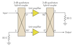
Many high-frequency LNAs have been designed and based on gallium-arsenide (GaAs) semiconductor technology for its noteworthy high gain and low noise at millimeter-wave frequencies.1-8 A balanced configuration offers numerous benefits in performance at these frequencies, with a typical balanced amplifier configuration consisting of two identical unit amplifiers and two quadrature hybrid couplers (Fig. 1). Input signals are split into quadrature signals by a coupler and fed to the two unit amplifiers. A coupler at the output combines the outputs of the two unit amplifiers.
At the input of the balanced amplifier, reflected signals from the two unit amplifiers are 180° out of phase and cancel each other out. For the same reason, at the output of the balanced amplifier, reflected signals will also be canceled, resulting in good input and output return-loss behavior for the balanced amplifier. The balanced amplifier also provides better stability compared to a single-ended amplifier.9-11 In a balanced amplifier, each unit amplifier is terminated with a fixed load, which is close to 50 Ω. So the actual loads at the input and output of the balanced amplifier only minimally affect the loads of the two unit amplifiers. Instead, the single-ended amplifier is affected by actual loads.
The amplifier may be unstable in some frequency ranges, especially if the actual load is a filter. A filter behaves as a 50-Ω load only in the passband. In the stopband, the filter will behave as a purely reactive load to the amplifier. The purely reactive load can cause the single-ended amplifier to become unstable. Furthermore, the failure of one unit amplifier will only cause a gain drop of 6 dB instead of catastrophic failure for the balanced amplifier.
To demonstrate the use of this balanced amplifier design approach, an LNA was designed based on a 0.15-μm GaAs pHEMT process. By employing more amplifier stages, the LNA exhibits a higher gain than the previous balanced LNAs.1,5 The input and output return losses of the LNA are improved by using two optimized Lange couplers at the RF input and output ports, respectively.
With application of a self-bias technique, the LNA can be biased from a single power supply. The LNA exhibits high gain of more than 34 dB with gain flatness within 0.8 dB, and a noise figure of less than 2.6 dB from 30 to 36 GHz. The LNA is stable at any frequency within its operating range.
Active devices for the LNA are grown on 6-in. GaAs substrates using a commercial 0.15-μm pHEMT process. The process provides GaInAs/AlGaAs pHEMT devices, using electron-beam lithography to define 0.15-μm T-gates. The low-noise pHEMTs consist of single-sided doped structures with a single recess. Connections are made by means of air bridge or slot viahole connections.
The process achieves devices with peak transconductance (gm) of 550 mS/mm at a gate-drain voltage of -0.1 VDC, a gate-drain breakdown voltage of +9 VDC, and a threshold voltage of -0.45 VDC. The process delivers devices with transition frequency, ft, of 95 GHz, and maximum frequency of oscillation, fmax, of 160 GHz.
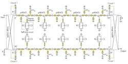
Low input and output return loss can be achieved by means of Lange couplers at the LNA’s input and output ports. Each of the LNA’s unit amplifier’s incorporates five common-source field-effect transistors (FETs), combining to form the balanced monolithic Ka-band amplifier shown in Fig. 2. The active devices are all 2 × 40 μm. The input matching networks of the first two amplifier stages were designed for optimum noise match for low noise figure, while the remaining amplifier stages were conjugate-matched for increased gain. The output matching networks were conjugate-matched for high gain.
Since the input and output return losses depend on the Lange couplers, the two unit amplifiers were optimized for gain, gain flatness, and noise figure. To bias the LNA from a single power supply rail, a self-bias circuit, consisting of a bypass capacitor (C2) and a resistor (R2), was used. For the best noise figure, bias voltages were selected to ensure that the amplifier operates in its low-noise region.
The drain-source voltage (Vds) and the gate-source voltage (Vgs) were selected at +2 VDC and -0.19 VDC, respectively, with the aid of computer software simulations. The source current was selected at 12.7 mA, so that resistors (R2 were chosen with value of 15 Ω to set a gate-source voltage (Vgs) of -0.19 VDC.
This file type includes high resolution graphics and schematics when applicable.
Coupler Concerns
This file type includes high resolution graphics and schematics when applicable.
Lange couplers, which readily provide broadband, 90-deg. phase splits of input signals, are detailed in design and operation in refs. 12 and 13. The Lange coupler for the current amplifier was designed with four fingers for use from 29 to 37 GHz, exceeding the frequency range (30 to 36 GHz) actually required by the LNA.
The coupler was computer-simulated with the aid of a commercial, three-dimensional (3D) electromagnetic (EM) simulation program. The simulated results of the Lange coupler indicate insertion loss of better than 3.52 dB, with amplitude balance of less than 0.48 dB and phase balance of less than 0.53 deg. from the reference 90-deg. phase difference.
For a pHEMT device, the load reflection coefficient, Γopt, is generally much different than S11*, the conjugate reflection coefficient of S11. This implies that an amplifier that is designed for minimum noise figure would also be mismatched for a maximum power-transfer condition.
However, by choosing an appropriate transistor size—and using series inductive feedback circuits at the source electrode of the pHEMT devices—it may be possible to achieve values of Γopt and S11*that are somewhat closer together, resulting in better output-power performance while still achieving low noise figure.
The source inductor is formed by inserting one transmission line, with length Ls, between the source electrode of the pHEMT and the self-bias circuit (Fig. 2). The values of Γopt and S11* are then calculated as a function of line length Ls and the gate width of the pHEMT device at 33 GHz to find the optimum values of Ls and gate width for best noise figure and output power. This analysis approach led to the selection of a gate width of 2 × 40 μm and line length Ls of 80 μm.
Gain flatness is an important specification in radar and communication systems,14,15 and the gain flatness for this LNA was targeted for performance within 0.8 dB. Gain flatness is limited by different active device characteristics, such as maximum available gain (MAG). Normally, MAG decreases linearly as frequency increases.
As a result, highpass reactive matching circuits are adopted for the input and output matching networks to compensate. The matching networks provide an upward frequency slope to compensate for the gain rolloff of the pHEMT devices, resulting in flat gain performance from 30 to 36 GHz.
LNA stability is another critical design consideration. By using a balanced topology, the stability of the LNA is better than the stability of the single-ended LNA. Due to the large gain characteristics of pHEMT devices in the lower frequency range, the LNA is more likely to have stability problems in this frequency band. Therefore, a low-loss resonator-type circuit is adopted to stabilize the LNA.
The stabilization circuit, consisting of a transmission line and a resistor (R1), as shown in Fig. 2 (circuit 1), has a weak resonance in the vicinity of 20 GHz. Resistor R1 acts as a dumping resistor at around 20 GHz to reduce the gain of the LNA in this frequency band. At the same time, this circuit does not degrade the LNA’s noise and gain performance levels within its target operating frequency range.
The Rollet’s condition, as defined in Eqs. 1-3:16
K = [1 - |S11|2 - |S22|2 + |Δ|2]/2|S12S21| > 1 (1)
b = 1 + |S11|2 - |S22|2 - |Δ|2 > 0 (2)
Δ = S11S22 – S12S21 (3)
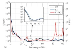
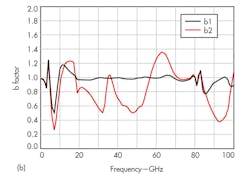
is used to check the stability of the LNA. When these two conditions are simultaneously satisfied, the LNA will be unconditionally stable. The simulated stability factor is shown in Fig. 3. Parameters K1 and b1 are stability factors for the whole LNA, while parameters K2 and b2 are stability factors for the unit amplifier. Parameters K1 and K2 are maintained above 1, while parameters b1 and b2 are maintained over 0 for the frequency range of 0 to 100 GHz, implying that the LNA will effectively be stable at any frequency. Meanwhile, parameter K1 is greater than K2 in all frequency ranges, indicating the better stability of the balanced amplifier compared to a single-ended amplifier.
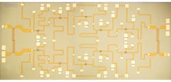
The designed five-stage balanced LNA was fabricated by a commercial 0.15-μm pHEMT semiconductor process, with a microphotograph of the chip shown in Fig. 4. The LNA chip measures 4.3 × 1.9 mm. Its noise figure and S-parameters were measured at room temperature while the device was still on wafer (using commercial wafer probes and associated test equipment).
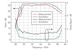
Figure 5 shows the simulated and measured noise figures and associated gains for the LNA. The gain is greater than 34 dB with 0.8 dB gain flatness from 30 to 36 GHz. The noise figure is less than 2.6 dB for the same bandwidth. The simulated and measured results are in close agreement.
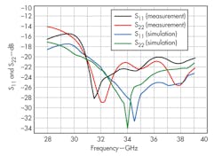
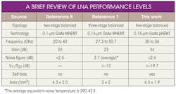
Figure 6 shows the simulated and measured input and output reflection coefficients, S11 and S22. The input and output return losses were found to be greater than 19.7 dB from 30 to 36 GHz, showing the effectiveness of the amplifier’s input and output matching networks. As the table shows, the LNA compares well with recently reported GaAs-based balanced LNAs.1,5
Its gain is greatly improved by the five-stage cascade structure, while its chip area was not significantly increased by its layout. It has a beneficial dual-Lange-coupler design and makes effective use of self-biasing and a single power supply, for ease of installation in a number of different applications.
This file type includes high resolution graphics and schematics when applicable.
Acknowledgment
This file type includes high resolution graphics and schematics when applicable.
This work was supported by the National Natural Science Foundation of China (Grant No. 61006026).
Ziqiang Yang, Associate Professor
Shaoteng Chi, Master’s Degree Candidate
Tao Yang, Professor
Yu Liu, Associate Professsor
Hao Peng, Ph.D.
School of Electronic Engineering, University of Electronic Science and Technology of China,
Chengdu 611731, People’s Republic of China
References
1. S.H. Weng, W.C. Wang, H.Y. Chang, C.C. Chiong, and M.T. Chen, “A Cryogenic 30-50 GHz balanced low noise amplifier using 0.15-μm MHEMT process for radio astronomy applications,” in IEEE 2012 International Symposium on RFIT, 2012, pp. 177-179.
2. D.M. Kang and H.S. Yoon, “80-110 GHz MMIC amplifiers using a 0.1-μm GaAs-based mHEMT technology,” Microwave and Optical Technology Letters, Vol. 54, No. 8, 2012, pp. 1978-1982.
3. C.M. Hu, C.Y. Huang, C.H. Chu, D.C. Chang, Y.Z. Juang, J. Gong, C.F. Huang, and C.M. Chin, “A 60-GHz three-stage low noise amplifier using 0.15-μm gallium-arsenide pseudomorphic high-electron mobility transistor technology,” Microwave and Optical Technology Letters, Vol. 54, No. 2, 2012, pp. 329-332.
4. Y.S. Lin and S.S. Wong, “A 60-GHz low-noise amplifier for 60-GHz dual-conversion receiver,” Microwave and Optical Technology Letters, Vol. 51, No. 4, 2009, pp. 885-891.
5. W.R. Deal, M. Biedenbender, P. Liu, J. Uyeda, M. Siddiqui, and R. Lai, “Design and Analysis of Broadband Dual-Gate Balanced Low-Noise Amplifiers,” IEEE Journal of Solid-State Circuits, Vol. 42, No. 10, 2007, pp. 2107-2115.
6. P.J. Riemer, B.R. Buhrow, J.B. Hacker, J. Bergman, B. Brar, B.K. Gilbert, and E.S. Daniel, “Low-power W-band CPWG InAs/AlSb HEMT low-noise amplifier,” IEEE Microwave and Wireless Components Letters, Vol. 16, No. 1, 2006, pp. 40-42.
7. J.B. Hacker, J. Bergman, G. Nagy, G. Sullivan, C. Kadow, L. Heng-Kuang, A.C. Gossard, M. Rodwell, and B. Brar, “An ultra-low power InAs/AlSb HEMT Ka-band low-noise amplifier,” IEEE Microwave and Wireless Components Letters, Vol. 14, No. 4, 2004, pp. 156-158.
8. B. Aja, M.L. de la Fuente, J.P. Pascual, M. Detratti, and E. Artal, “GaAs pHEMT broadband low-noise amplifier for millimeter-wave radiometer, ” Microwave and Optical Technology Letters, Vol. 39, No. 6, 2003, pp. 475-479.
9. A.F. Osman and N.M. Noh, “Wideband LNA design for SDR radio using balanced amplifier topology,” in 4th Asia Symposium on Quality Electronic Design, 2012, pp. 86-90.
10. I. Malo-Gomez, J. D. Gallego-Puyol, C. Diez-Gonzalez, I. Lopez-Fernandez, and C. Briso-Rodriguez, “Cryogenic Hybrid Coupler for Ultra-Low-Noise Radio Astronomy Balanced Amplifiers,” Microwave Journal of Theory and Techniques, Vol. 57, No. 12, 2009, pp. 3239-3245.
11. Wantcominc.com, “Merits of balanced amplifier,” Application Note AN-101.
12. R.M. Osmani, “Synthesis of Lange Couplers,” IEEE Transactions on Microwave Theory & Techniques, Vol. 29, No. 2, 1981, pp. 168-170.
13. W.P. Ou, “Design equations for an interdigitated directional coupler,” IEEE Transactions on Microwave Theory & Techniques, Vol. 23, No. 2, 1975, pp. 253-255.
14. Y.H. Yu, Y.S. Yang, and Y.J. Chen, “A Compact Wideband CMOS Low Noise Amplifier With Gain Flatness Enhancement,” IEEE Journal on Solid-State Circuits, Vol. 45, No. 3, 2010, pp. 502-509.
15. D.H. Zhang, W.R. Zhang, D.Y. Jin, H.Y. Xie, X. Zhao, B.Y. Liu, and Y.Q. Zhou, “The feedback technology for gain flatness and stability of UWB LNA,” 2011 International Conference on Electric Information and Control Engineering, pp. 6260-6263 (2011).
16. G. Gonzalez, Microwave Transistor Amplifiers: Analysis and Design, Prentice-Hall, Inc., Englewood Cliffs, NJ, 1984.
This file type includes high resolution graphics and schematics when applicable.
About the Author

Leaders relevant to this article:
