This file type includes high resolution graphics and schematics when applicable.
Power amplifiers (PAs) for wireless local area network (WLAN) in the industrial-scientific-medical (ISM) band at 2.4 GHz are enabling high-speed wireless data communications in a wide range of locations, including homes, offices, and airports. WLAN radios working at ISM frequencies have provided data transmission speeds to 54 Mb/s, and this frequency band is becoming more and more crowded as the number of users grows.
To avoid loss of bandwidth and bit rates at 2.4 GHz, the unlicensed national information infrastructure (UNII) band at 5 GHz provides an alternative frequency range for WLAN radios. This higher-frequency band features 12 non-overlapping channels and can support data transmissions at 10 times the rates possible at 2.4 GHz. In support of 5-GHz WLANs, a power amplifier module (PAM) was developed with the aid of electromagnetic (EM) analysis techniques and broadband matching theory. It provides better than 1 W saturated output power from 4.9 to 5.9 GHz while operating on +3.3-V dc bias.
The IEEE has defined requirements for 5-GHz UNII-band WLANs by its IEEE 802.11ac standard.1 For PAs, the standard poses challenging requirements for vector-error-magnitude (EVM) performance for all operating conditions and flat gain across the band.2 At higher frequencies, implementing a PA that meets these requirements becomes difficult due to excessive characteristic capacitance and inductance of the PA circuit elements. However, by using EM analysis and wideband impedance matching, a high-output PAM was developed for WLAN applications. The amplifier achieves better than +29-dBm output power at 1-dB compression from 4.9 to 5.9 GHz.
The PAM consists of two parts: an InGaP/GaAs heterojunction-bipolar-transistor (HBT) monolithic-microwave-integrated-circuit (MMIC) amplifier device and a high-frequency circuit laminate. The laminate was simulated by means of three-dimensional (3D) EM models and EM analysis techniques. In the analysis of the EM models of inductors on the laminate or capacitors in the InGaP/GaAs HBT MMIC, some parasitic parameters are extracted to create simple equivalent circuits for the design of the broadband matching network. The laminate’s inductors consist of microstrip lines or bonding wires. Any parasitic capacitance from these inductors will complicate the creation of an impedance matching network for the PAM, since this capacitance will be part of the matching network.
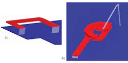
Figure 1 shows several 3D EM models—for the microstrip of an output matching network on the laminate in (a), as well as a bond wire and microstrip serving as the bias power inductance in (b). This microstrip transmission line serving as an inductor is different from an ideal inductor: It exhibits distributed capacitance between the transmission line and the ground. According to a differential model of the transmission line,3 an equivalent circuit was proposed to describe the parasitic characteristics of the inductor in Fig. 1(a); the parameters of this circuit can be extracted from EM simulation results. Equivalent circuits for Figs. 1(a) and (b) are shown in Figs. 2(a) and (b).
The inductor in Fig. 1(a) can be considered a two-port network. Using EM analysis, the network’s S- and Y-parameters can be found over a wide frequency range. The parameters of the equivalent circuit in Fig. 2(b) also can be found through EM simulation.
The inductor in Fig. 1(a) can be regarded as a two-port network. Using the electromagnetic techniques described above, the S-parameters and Y parameters of this network can be obtained over a wide frequency range. After the electromagnetic simulation, the parameters of the equivalent circuit in Fig. 2 (b)—which describe the frequency characteristic of the inductors—can be calculated from the Y parameters. According to the definition of Y-parameters, Eq. 1 can be obtained from Fig. 2(b), and the parameters in Fig. 2(b) can be calculated using Eqs. 1 and 2:
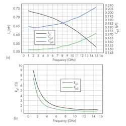
The parameters in Fig. 2(b) for the inductor of Fig. 1(a) are shown from 1 to 15 GHz in Figs. 3(a) and (b). The effective inductance, Ls, decreases and the parasitic capacitances Cp1 and Cp2 increase with increasing frequency, which demonstrating that the frequency-dependent parasitic characteristics of inductors should be taken into account in the high-frequency range. The frequency-dependent parasitic characteristics of the power bias inductor in Fig. 1(b) also can be evaluated by the equivalent circuit in Fig. 2(b) following EM simulation.
The capacitor in the MMIC also contributes to parasitic circuit elements in the PAM. Figure 4(a) shows a cross-sectional view of a stacked capacitor in the InGaP/GaAs HBT MMIC while Fig. 4(b) details its 3D EM model. At frequencies below 1 GHz, the parasitic capacitance of this capacitor can be ignored since the effective low-frequency capacitance of this circuit element is the same as its DC capacitance.
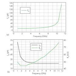
Based on EM simulation, the effective capacitance of this component increases in the UNII band. When the frequency exceeds the cutoff frequency of the capacitor, it works like an inductor. Figure 5 offers a simple equivalent circuit for the component in Fig. 4(b). Figure 6 shows the values for the circuit elements in this equivalent circuit from 1 to 11 GHz, based on EM simulation.
The DC capacitance of the capacitor component in Fig. 4(b) is 9 pF in this InGaP/GaAs HBT process, as confirmed by many designs below 1 GHz. The effective capacitance increases to about 11 pF at 5 GHz, according to the EM simulation results in Fig. 6(a). When the frequency increases to 8 GHz, the effective capacitance is about 30 pF since parasitic inductor Ls dominates at these higher frequencies. The value of Ls is almost the same from 4 to 11 GHz—about 20 pH.
In addition, the electrical connections to the capacitor of Fig. 4(b) add more parasitic inductance, making implementation of a matching network more difficult. However, this complexity can be solved through the use of EM analysis techniques. EM analysis makes it possible to account for the parasitic elements of the various passive components in the PAM’s matching networks in great detail.
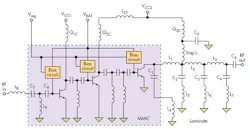
Figure 7 offers a schematic circuit diagram of a three-stage PA with inductors and capacitors not having high-frequency parasitic characteristics. Without the high-frequency parasitic characteristics, the schematic circuit diagram serves only as a guideline for the design parameters of each circuit element. More precise values can be obtained by means of EM analysis.
This file type includes high resolution graphics and schematics when applicable.
Achieving the Amplifier
This file type includes high resolution graphics and schematics when applicable.
For 5-GHz WLAN use, the PAM was designed for operation from 4.9 to 5.9 GHz; its 1-GHz bandwidth will satisfy the requirements of the IEEE 802.11ac standard. To obtain low EVM, the output 1-dB compression point should be suitably high and the power gain should be flat, with minimal phase distortion to the 1-dB compression point. In this design, diode-based linearizing bias techniques4-6 have been used to improve linearity. With +3.3-V dc bias, the impedance of the output matching network must be low enough over the 1-GHz bandwidth to achieve saturated output power7 greater than 1 W. The output matching network is designed on the laminate according to Fig. 7 using EM techniques.
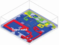
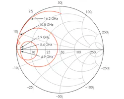
Figure 8 shows the EM model of the laminate without surface-mount capacitors, but with the addition of high-frequency parasitic characteristics. Figure 9 offers the EM-simulated impedance of the output matching network to the HBTs; the fundamental impedance is about 2.5 Ω from 4.9 to 5.9 GHz, a low-enough value to attain the desired saturated output power for the PAM. The insertion loss of the output matching network is also less than 0.5 dB across the 1-GHz bandwidth.
The input matching network and interstage matching networks were designed on the MMIC to save area on the laminate. They consist of several L-type transformers to ensure a bandwidth of 1 GHz. The DC capacitances of the capacitors on the MMIC are less than the guidelines set in Fig. 7. In conjunction with the parasitic inductances produced in or around the actual capacitors, the effective capacitance in Fig. 7 is obtained in the high-frequency range, according to EM analysis. With this design approach, the DC capacitance of the capacitors in the MMIC can be determined from EM simulation results, which include the high-frequency parasitic characteristics.
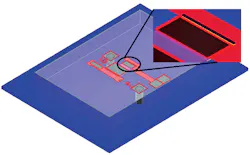
Figure 10 shows an EM model of an interstage matching network between the PAM’s middle and output stages in the MMIC; the simulated function is the same as the matching network in Fig. 7, but the DC capacitances of the capacitors in Fig. 10 are less than the effective capacitances in Fig. 7.
Figure 11 shows the fabricated PAM. It consists of a PA MMIC, several surface-mount capacitors, and bond wires on a microwave laminate. The PAM measures 4 × 4 mm, which is the size of the laminate; the InGaP/GaAs HBT MMIC itself measures 1000 × 700 μm. The emitter area of the output stage is 4800 μm2 and the emitter areas of the first- and second-stage HBTs are 960 and 480 μm2, respectively. The input matching network consists of two capacitors, an inductor in the MMIC, a bond wire, and microstrip transmission lines on the laminate. The output matching network is formed by four bond wires and several surface-mount capacitors connected to inductors on the laminate.
Figure 12 presents the measured S11, S21, and S22 parameters for the PAM, measured with continuous-wave (CW) signals. The peak value for S21 is about 28.3 dB at 5.3 GHz. The small-signal gain for the PAM fluctuates within a 2-dB window across the frequency range, while S22 is less than -10 dB from 4.9 to 5.9 GHz.
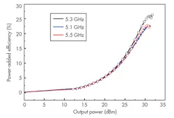
Figure 13 depicts the dependence of the power gain on the output power of the PAM at +3.3-V dc bias at 5.1, 5.5, and 5.7 GHz. The saturated output power is greater than +31 dBm and the power gain is greater than 27 dB at all three frequencies. The saturated output power is greater than +30 dBm at 4.9, 5.7, and 5.9 GHz. The output 1-dB compression point is greater than +29 dBm from 4.9 to 5.9 GHz. The measured dependence of PAE on output power at 5.1, 5.3, and 5.5 GHz is plotted in Fig. 14, where PAE reaches 26.5% at 5.3 GHz.
Zheng Ruiqing, Senior Design Engineer
Zhang Guohao, Design Engineer
Zhang Zhihao, Design Engineer
Guangdong University of Technology, School of Information Engineering, Guangzhou 510006, PRC; +86-13450222131
This file type includes high resolution graphics and schematics when applicable.
References
This file type includes high resolution graphics and schematics when applicable.
1. IEEE 802.11: “Wireless LAN Medium Access Control (MAC) and Physical Layer (PHY) Specifications (2012 revision),” IEEE Standards Association, March 29, 2012; K. Kurokawa, “Design theory of balanced transistor amplifiers,” The Bell System Technical Journal, Vol. 44, October 1965, pp. 1675-1698.
2. Yazhou Wang and Randy Naylor, “Challenges in Designing 5 GHz 802.11ac WiFi Power Amplifiers,” in Wireless Connectivity Business Unit, RF Micro Devices, Inc., Billerica, MA 01821.
3. Reinhold Ludwig and Pavel Bretchko, “RF Circuit Design: Theory and Applications,” America, 2002, pp.360-362.
4. T. Yoshimasu, M. Akagi, N. Tanba, and S. Hara, “An HBT MMIC power amplifier with an integrated diode linearizer for low-voltage portable phone applications,” IEEE Journal of Solid State Circuits, Vol. 33, No. 9, September 1998, pp. 1290-1296.
5. H. Kawamura, K. Sakuno, T. Hasegawa, M. Hasegawa, H. Koh, and H.Sato, “A miniature 44% efficiency GaAs HBT power amplifier MMIC for the W-CDMA application,” in 22nd IEEE GaAs IC Symposium Technical Digest, Seattle, WA, November 2000, pp. 25-28; M. Young, “The Technical Writers Handbook,” University Science, Mill Valley, CA, 1989.
6. H. Koh, K. Sakuno, H. Kawamura, Y. Amano, M. Hasegawa, K. Kagoshima, K. Shirakawa, N. Takahashi, Y. Liu, T. Oka, K. Fujita, M. Yamashita, N. Matsumoto, and H. Sato, “A high efficiency InGaP/GaAs HBT power amplifier MMIC for the 5 GHz wireless-LAN application,” in Proceedings of the 32nd European Microwave Conference, Milan, Italy, September 2002, pp. 469-472.
7. Steve C. Cripps, RF Power Amplifiers for Wireless Communications, Artech House Publishers, Norwood, MA, 2006.
This file type includes high resolution graphics and schematics when applicable.


