What’s the State of GaN Power Amplification?
This file type includes high resolution graphics and schematics when applicable.
Gallium-nitride (GaN) power semiconductor technology has helped significantly improve performance levels in RF/microwave power amplification. By reducing device parasitic elements and using shorter gate lengths, and using higher operating voltages, GaN transistors have reached higher output-power densities, wider bandwidths, and improved dc-to-RF efficiencies.
For example, by 2014, GaN-based X-band amplifiers capable of 8-kW pulsed output power were demonstrated for radar systems applications as replacements for traveling-wave-tube (TWT) devices and TWT amplifiers. By 2016, we expect to see 32-kW variants of these solid-state GaN power amplifiers. In anticipation of these high-power GaN amplifiers, it’s probably a good idea to review some of their key characteristics and features.
In the recent past, GaN has been the technology of choice for counter-radio-frequency electronic warfare (CREW) applications with tens of thousands of amplifiers delivered for field use. The technology is now being deployed in the airborne EW arena as well, with amplifiers under development able to deliver hundreds of watts of output power across multiple octaves in the RF/microwave range. Several variants of these wideband EW power amplifiers are due for release in the current calendar year.
Areas for further research include improvements in linearity for high peak-to-average-power-ratio (PAPR) waveforms employed in many military communications systems, including common data link (CDL), wideband networking waveform (WNW), soldier radio waveform (SRW), and wideband satellite-communications (satcom) applications. Along those lines, Analog Devices is pursuing the “Bits to RF” initiative, which integrates the company’s strengths in baseband signal-processing and GaN power-amplifier (PA) technologies. This integration will enable advances in PA linearity and efficiency via techniques such as predistortion and envelope modulation.
The Advent of GaN in High-Power Amps
In the last few years, GaN-based devices, both discrete field effect transistors (FETs) and monolithic microwave integrated circuits (MMICs), have been released and widely used in high-power microwave amplifier systems. Available from several foundry sources and device manufacturers, they’re typically fabricated on 100-mm silicon-carbide (SiC) wafers. GaN-on-Si processes are also under consideration; however, the relatively poor thermal and electrical conductivities of Si offsets the cost advantages in high-performance, high-reliability applications.
GaN-based devices feature gate lengths as small as 0.2 µm and support operation into millimeter-wave frequency bands. Such devices have largely replaced gallium arsenide (GaAs) and Si laterally diffused metal-oxide-semiconductor (LDMOS) devices in high-frequency applications and all but the most cost-sensitive, lower-frequency applications.
RF power-amplifier designers are attracted to GaN devices because they support very high operating voltages (three to five times higher than those of GaAs), and roughly double the allowable current per unit FET gate width compared to GaAs devices. These characteristics have an important consequence to PA designers, specifically a higher load impedance for a given output power level.
Previous GaAs- or LDMOS-based designs often had extremely low output impedances relative to typical system impedances of 50 or 75 {CAP OMEGA}. Low device impedances place limits on achievable bandwidth. In other words, as the required impedance transformation ratio between the amplifying device and its load increases, the number of components and insertion loss increase as well. Due to these high impedances, early users of these devices sometimes were able to achieve partial results by merely installing one in an unmatched test fixture, applying dc bias, and driving the device with an RF/microwave test signal.
GaN devices are also finding their way into high-reliability space applications due to these operating characteristics and their exceptional reliability. Life test data from several sources of these devices predict mean-time-to-failure (MTTF) durations (for single devices) in excess of one million hours at junction temperatures of 225{DEG}C or higher. This exceptional reliability is mainly due to the high bandgap value for GaN (3.4 for GaN vs. 1.4 for GaAs). This makes them more than suitable for high-reliability applications.
Cost Implications
The chief impediment to wider use of GaN in high-power applications has been its relatively high fabrication costs—typically two to three times that of GaAs and five to seven times that of Si LDMOS-based devices. It’s become a barrier for cost-sensitive applications such as wireless infrastructure and consumer handsets.
GaN-on-Si-substrate processes are available, albeit with the performance issues noted earlier. Nonetheless, devices from these processes are probably best suited for these cost-sensitive applications. In the near future, cost reductions, perhaps on the order of 50%, are expected as GaN-device fabrication moves to larger wafers—several leading foundries in this realm are now developing wafers with diameters of 150 mm and larger.
Currently deployed radar systems for weather prediction and target acquisition/identification rely on TWT-based power amplifiers operating at C- and X-band frequencies. The amplifiers run at high supply voltages (10 to 100 kV), and temperatures and are susceptible to damage from excessive shock and vibration. The reliability in the field for these tube-based amplifiers is typically 1200 to 1500 h, which leads to high costs for maintenance and for spare parts.
GaN-Based Option to TWT Amps
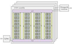
As an alternative to these high-power TWT-based amplifiers, Analog Devices developed an 8-kW solid-state X-band power amplifier based on GaN technology. The design uses an innovative, layered combiner approach to sum the contributed RF/microwave output power of 256 MMICs, each developing approximately 10 W output power. The combining methodology results in graceful performance degradation in the event of individual MMIC failures.
Conversely, TWT amplifiers tend to suffer catastrophic-type failures due to low levels of redundancy. For these GaN solid-state power amplifiers (SSPAs), the RF/microwave combining architecture must present a reasonable balance between the isolation required between MMICs and the RF/microwave insertion loss of the overall network.
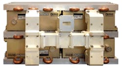
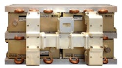
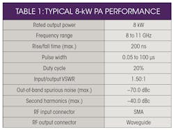
The 8-kW amplifier topology is modular; it combines the output power of four 2-kW amplifier assemblies using waveguide structures (Fig. 1). The amplifier can be mounted in a standard 19-in. rack enclosure. The amplifier’s design is configured for water cooling (Fig. 2), although variants of the amplifier using air cooling are under development. Table 1 summarizes the performance levels for the water-cooled 8-kW GaN PA.
Due to their modular design, the 8-kW SSPAs can be combined to produce even higher power levels. Work is underway to develop an amplifier that will combine three of these 8-kW SSPA modules to achieve a unit with a peak output-power level of 24 kW across the same frequency range. Other configurations that achieve power levels to 32 kW are feasible and being considered for further evaluation.
In another development, Analog Devices is working on an advanced power module, also based on GaN technology, that will double the RF/microwave output power of current modules. Intended to be hermetically sealed, it will support operation in extreme environments. This, along with next-generation combining structures with reduced insertion loss (compared to current approaches), will extend pulsed output power to levels approaching 75 to 100 kW at RF/microwave frequencies. These advanced, high-power SSPAs will include control and processor functionality to enable fault monitoring, built-in-test (BIT) functionality, remote diagnostic testing, and control of fast, real-time bias control circuits for the MMIC devices that power the amplifiers.
The GaN-based SSPAs address the industry’s need for amplifiers with wide instantaneous bandwidths and high output-power levels. Some systems attempt to meet these requirements using “channelized” or multiple amplifiers each covering a portion of the required spectrum and feeding a multiplexer. This increases cost and complexity and results in coverage gaps at the frequency crossover points of the multiplexer. A more effective, alternative solution leverages continuous coverage of wide frequency ranges at elevated power levels, as was accomplished with two different GaN-based amplifiers covering VHF through L-band frequencies as well as 2 to 18 GHz.
Amp Varieties
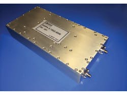
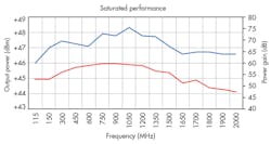
For VHF through S-band frequencies, Analog Devices developed a very small, feature-rich, multiple-octave amplifier capable of 50-W output power from 115 to 2000 MHz. The amplifier achieves output-power levels of +46 dBm (typically 40 W) across that full frequency range when fed with a nominal input signal of 0 dBm. Packed in a compact housing with dimensions of 7.3 × 3.6 × 1.4 in., the amplifier includes BIT functionality for thermal and current overload protection, telemetry reporting, and an integrated dc-dc converter for uncompromised RF performance with input supplies ranging from +26 to +30 V dc. Fig. 3 provides a photograph of the amplifier, and Fig. 4 presents typical measured performance data for output power versus frequency.
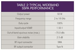
To address wideband applications above 2 GHz, the company also developed a GaN amplifier that produces 50-W continuous-wave (CW) output power across the entire 2- to 18-GHz band. This amplifier uses commercially available 10-W GaN MMICs with output-power contributions summed by means of a wideband, low-loss combiner circuit. Multiple amplifiers may in turn be combined to develop output power as high as 200 W across this same 2- to 18-GHz bandwidth. The driver amplifier chain is also based on GaN active devices.
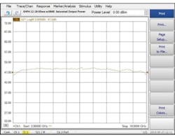
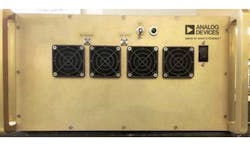
The device operates from +48 V dc and features an internal voltage regulator and high-speed switching circuits to enable pulsed operation with good pulse fidelity and fast rise and fall times. Table 2 lists the amplifier’s (depicted in Fig. 5) specifications; while Fig. 6 presents the amplifier’s output power as a function of frequency from 2 to 18 GHz.
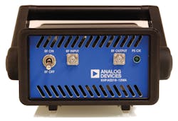
This 50-W amplifier is one of a family of amplifiers covering the 2-to-18-GHz band. The firm also crafted a compact, benchtop amplifier capable of 12-W output power (Fig. 7) and a rack-mount unit that offers 100-W output power (Fig. 8). Other amplifiers, with frequency coverage from 2 to 6 GHz and 6 to 18 GHz, are under development.
On top of that, Analog Devices is attempting to increase the output power of these broadband amplifiers from their present levels to power levels of 200 W and higher. To achieve these higher output-power levels, the company is working on modules with increased output power as well as broadband RF power combiners with much-improved combining efficiency and less loss than current power combiners.
These represent a few examples of the performance levels possible with GaN-based solid-state amplifiers. Unit costs of the amplifiers are expected to decrease as more GaN semiconductor vendors move to larger wafer sizes and continue to improve their yields of devices per wafer. Systems operating at millimeter-wave frequencies will see greater use of GaN devices as gate lengths are reduced, enabling higher frequency operation for GaN-based SSPAs. It’s clear that current GaN trends of improving performance and dropping costs will continue for some time.
Walt DeMore is an Engineering Manager at Analog Devices Inc.
