GaN: From Esoteric Tech to Market Mainstay
This file type includes high-resolution graphics and schematics when applicable.
The evolution of gallium nitride (GaN) from research and development to commercial deployment is the single largest technology disruption impacting the RF/microwave industry today. GaN has had a clear and profound effect on system performance, size, and weight across numerous RF applications, enabling system-level solutions that couldn’t be achieved with legacy semiconductor technologies. Still, GaN’s market potential has only just begun to be realized.
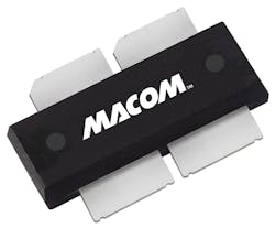
Today, GaN is positioned for mainstream adoption in commercial RF applications spanning from wireless base stations to RF energy and beyond (Fig. 1). Its trajectory has hinged on a wide range of factors coming into alignment, though.
For example, GaN’s performance benefits were once prohibitively expensive. However, a number of recent advances have distinguished GaN as the cost-competitive successor to gallium arsenide (GaAs) and laterally diffused metal-oxide semiconductor (LDMOS) technology for most RF applications. These advances include GaN-on-silicon (GaN-on-Si) technology, supply-chain optimization, device packaging techniques, and manufacturing efficiencies.
A better perspective on where GaN technology is today and where it’s headed in the future can be drawn by reflecting on its origins and development roadmap. In many respects, GaN’s evolution is an example of history repeating itself.
The Formative Years
The U.S. Department of Defense (DoD) played a pivotal role in the development of GaAs-based monolithic microwave integrated circuits (MMICs) some 20+ years ago via the Microwave/Millimeter-Wave Monolithic Integrated Circuits (MIMIC) and Microwave Analog Front-End Technology (MAFET) programs. The DoD was equally instrumental in the early development of GaN by way of the Defense Advanced Research Projects Agency’s (DARPA) Wide Bandgap Semiconductor Technology (WBST) initiative. Officially launched in 2001, this initiative sought to fulfill the military’s need for compact, high-power RF devices, building in part on the early success demonstrated by GaN for blue-spectrum LED lighting.
Aimed at fast-tracking GaN’s use in military systems, the WBST initiative chartered program participants to cultivate MMIC fabrication processes for reproducible GaN devices with predictable performance characteristics and failure rates. As with the MIMIC and MAFET programs that preceded it, the WBST initiative was heavily skewed toward military applications that required performance at any cost. However, it would ultimately ensure the government’s access to increasingly affordable, high-performance RF components as compound semiconductor providers honed their process disciplines.
For GaAs, the catalyst for mainstream commercial adoption was the explosion in consumer demand for wireless handsets, which drove strong economies of scale. Compound semiconductor providers led the industry toward the establishment of robust, reliable, and scalable GaAs supply chains, investing hundreds of millions of dollars in large-scale GaAs fabs. Making that move enabled GaAs’ transition from specialized military technology to commercial mainstay.
GaN’s commercial adoption commenced primarily in the cable TV (CATV) industry, driven by operators’ desire to increase bandwidth while simultaneously reducing operating costs via improved energy efficiency. Despite GaN-on-silicon-carbide’s (GaN-on-SiC) price premium compared to GaAs, price pressures for CATV infrastructure were more relaxed than those for wireless handsets, and the operating cost savings overrode the jump in acquisition cost. But the volume benefits of the commercial CATV market would be counterbalanced by steepening price-erosion curves, which intensified efforts to cultivate cheaper alternatives to GaN-on-SiC.
The performance gap between GaN-on-SiC and GaN-on-Si has narrowed considerably since the early stages of CATV adoption, yielding cost-effective GaN-on-Si power transistors that now have similar power efficiency and thermal attributes to GaN-on-SiC. MACOM’s fourth-generation GaN-on-Si (Gen4 GaN) exemplifies this trend, delivering greater than 70% peak efficiency and 19-dB gain for continuous-wave (CW) operation from 2.45 to 2.7 GHz (Fig. 2).
In the wireless base-station market, this performance profile has enabled GaN to challenge LDMOS’ multi-decade dominance in base-station power amplifiers (PAs). Such a shift has profound implications for base-station performance and operating costs. The clear technology advantages provided by GaN—such as improved energy efficiency, greater bandwidth, higher power density, and smaller form factors—position it as the natural successor to LDMOS for next-generation base stations (particularly for cellular bands above 1.8 GHz).
Performance Advantages
When assessing GaN’s technology trajectory and market potential, one must of course weigh the baseline technical merits that distinguish GaN from legacy semiconductor technologies. The performance attributes of both GaAs and LDMOS—measured in power, efficiency, bandwidth, and thermal stability—were adequate for their target applications. But among their most noteworthy shortcomings were GaAs being limited to a power output below 50 W and LDMOS limited to frequencies below 3 GHz.
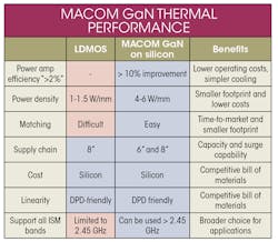
While the power and frequency capabilities of GaAs and LDMOS are compromised, GaN demonstrates exceptional performance across both of these metrics in addition to offering several other technical benefits (see table). GaN delivers considerably higher raw power density than incumbent GaAs and LDMOS technologies, with the capability of scaling the device technology to high frequency. GaN technology has allowed device designers to achieve broad bandwidths while maintaining high efficiency—more than 10 percentage points greater than LDMOS. When properly exploited, this efficiency delta can have a big impact at the system level in commercial applications.
Competing Costs
GaN’s performance benefits are well known to all involved with the RF/microwave industry. But its historical cost structure made it prohibitively expensive, which slowed its mainstream adoption. This is no longer the case, though, and customers’ perceptions and expectations for GaN are evolving accordingly.
Taking into account the inherent power-density advantage and scalability to 8-in. substrates, Gen4 GaN is expected to yield GaN-based devices that are more cost-effective than LDMOS in absolute dollars-per-watt before even considering the benefits at a system level. Gen4 GaN provides significantly lower cost than comparably performing, but more expensive, GaN-on-SiC wafers at volume production levels.
What’s more, the industry’s ability to support commercial-scale production of GaN-on-Si, maintain inventories, and accommodate surges in demand is now firmly established. Thus, concerns about supply scarcity have diminished—concerns that will continue to linger with GaN-on-SiC given its cost- and time-intensive fabrication process.
The parallel advances in the GaN technology roadmap and GaN supply chain have enabled the manufacturing scale and cost structures necessary to allow GaN to accelerate its penetration into commercial domains. For customers evaluating where GaN does and doesn’t fit based on performance and cost metrics, Gen4 GaN has changed the equation considerably.
Packaging and Manufacturing Efficiency
GaN packaging options are an essential part of its value proposition, with implications for product performance and cost, as well as manufacturing efficiency. Ceramics remain the packaging option of choice for GaN devices that must be hermetically sealed in order to ensure reliable operation over very long lifecycles. GaN in ceramic devices are also capable of managing high-power dissipation levels. The clear downside of leveraging GaN in ceramic components, however, is the high cost of the package and their cumbersome assembly processes. This extra touch labor adds considerably more cost.
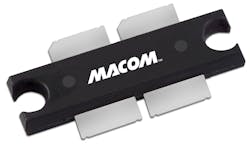
The GaN device market shifted radically with the introduction of GaN in plastic power transistors, which offer a cost-effective alternative to GaN in ceramic devices and are key to enabling a new generation of high-power, ultra-compact power modules (Fig. 3). Plastic-packaged, high-power GaN devices allow designers to adopt conventional surface-mount manufacturing approaches and their associated manufacturing efficiencies. In this way, the adoption of GaN in plastic further drives a roadmap for supply-chain cost reduction.
The Promise of RF Energy
The intersection of GaN performance with silicon cost structures is going to accelerate innovation across the RF domain, and open massive new market opportunities. Chief among them will be RF energy applications, which use controlled electromagnetic (EM) radiation to heat items or drive all kinds of processes. Today, magnetron tubes commonly generate this energy. Tomorrow, it will be generated by an all solid-state RF semiconductor chain.
Solid-state RF energy offers numerous benefits unavailable via alternate solutions: low-voltage drive, semiconductor-type reliability, smaller form factor, and an “all-solid-state electronics” footprint. Perhaps its most compelling attributes are fast frequency, phase, and power agility complemented by hyper-precision. Collectively, the technology’s attributes yield an unprecedented process-control range, even energy distribution, and fast adaption to changing load conditions.
RF energy is proving to be a highly efficient and precise heat and power source for a wide range of commercial applications, including microwave ovens, automotive ignition, and lighting systems, as well as industrial, scientific and medical (ISM) applications such as RF plasma lighting, material drying, and blood and tissue heating and ablation. The RF devices that underpin these systems must strike an optimal balance of performance, power efficiency, small size, and reliability—at a price point that promotes mainstream commercial adoption—and GaN-on-Si does just that. Rugged, plastic-packaged Gen4 GaN power transistors capable of up to 300-W power output have emerged as a compelling and cost-effective solution.
The wireless base-station market will continue to drive significant growth in the GaN market in the near term. Furthermore, now that GaN has crossed the threshold for mainstream adoption, it’s opening the door to another opportunity: RF energy applications.
The total addressable market for RF energy applications is enormous in scope. Consider the market for microwave ovens as just one example. MACOM estimates that more than 70 million microwave ovens are sold globally each year. With transmit powers for consumer units ranging from approximately 600 to 1,500 W, the total RF power demand for microwave ovens is in the 42- to 105-GW range. At current mainstream semiconductor price structures, the corresponding microwave-oven market revenue opportunity is approximately $4 to 9B.
GaN has come a long way since the DARPA WBST initiative, and its rise to the forefront of the RF/microwave industry is now complete. Its cost structure has come into alignment with legacy semiconductor technologies, and whenever cost parity is achieved between competing technologies, the higher-performing technology always wins.
The major investments made by companies like MACOM in this once burgeoning technology, and in its supply-chain ecosystem, set the stage for GaN’s mainstream commercial adoption. It will have a transformative impact on our industry and others for decades to come.
Mark Murphy works in marketing for RF Energy at MACOM.


