What you’ll learn:
- The complexity of the electronic-warfare landscape stresses RF front ends.
- The critical nature of half-wave element spacing in phased arrays.
- A 3D-stacked packaging approach shrinks switched filter banks without sacrificing RF performance.
Electronic warfare (EW) covers multiple disciplines including threat suppression, threat detection, and threat neutralization. The threat-detection aspect of EW requires the technology to listen for a wide variety of electromagnetic (EM) activity and make sense of it. This process involves collecting a swath of signals and translating them into the digital domain as efficiently as possible.
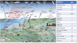
With technological advancement in the military environment and a drastic increase in the number of connected devices in circulation, the EW landscape is becoming increasingly complex and diverse. For example, consider the wide range of EM-reliant systems onboard an unmanned aerial vehicle (UAV)—a single element in the EW landscape (Fig. 1). For viable threat detection, EW systems need to function across the entire frequency spectrum, from VHF to Ku-band and beyond.
Unfortunately, an analog-to-digital converter (ADC) has no sympathy for this challenge. Every detectable signal (such as enemy radio, radar, and so on) needs to be converted into something an ADC is prepared to handle. How do you go about picking up frequencies across the spectrum? The short answer: Tuners have a lot of work to do.
Managing Ultra-Wideband Inputs
Tuner blocks are tasked with turning an unknown frequency into something predictable for the ADC, and the rest of the system, as efficiently as possible. The transition from RF to digital is shortened with direct sampling. S-band is traditionally the upper limit for this architecture, but it’s not fixed. Direct sampling at higher frequencies is right around the corner. However, at this point, anything above S-band requires a different tactic, such as a high intermediate-frequency (IF) approach.
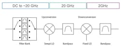
A common structure one might see in the tuner block is a two-stage conversion architecture (Fig. 2). In such an approach, a switched filter bank performs a pre-select function before upconverting to a fixed frequency, filtering at that frequency, and then downconverting to a suitable IF before filtering again. The pre-select allows designers to home in on the range they’re working with. Given the wideband nature of the input, the two-stage conversion method significantly reduces the frequency planning challenges (regarding factors such as spur placement) that a designer might encounter.
However, the pre-select stage presents a potential roadblock. Building a sufficiently high-performance switched filter bank that provides low loss and high selectivity is particularly challenging with strict size constraints. SWaP—size, weight, and power—is fundamental to success in defense and aerospace applications. Minimizing the footprint of a switched filter bank frees board space for additional functionality and reduces the weight of the RF system.
Beyond SWaP: Half-Wave Spacing
Rising out of a need for innovation in military radar-tracking applications, defense organizations were early adopters of beamforming technology and have supported its progress for several decades. As this technology becomes more popular and sophisticated, operational frequencies increase, and as described, the military faces a wider span of threat-detection targets.
Depending on the application, several different configurations exist for beamforming technology. An analog beamforming scheme uses a single ADC for the entire phased array. In this case, adjustments to the array are limited to the functionality of one ADC. Multiple beams can be supported with analog beamforming, but each additional beam requires a phase-adjustment channel; this arrangement typically increases cost and power consumption. That said, analog beamforming is better for low-consumption, low-beam-count systems.
For more flexibility, a hybrid beamforming approach employs digitally combined subarrays of analog beamforming. This is helpful for applications that would benefit from digital beamforming but can’t support fully digital beamforming due to practical constraints stemming from size and power consumption.
With fully digital beamforming, a dedicated ADC for each antenna element enables multiple beams to be acquired and transmitted simultaneously. This configuration improves dynamic range, drastically expanding the number of signals that can be detected.
Due to the complex landscape of signals to assess, such a configuration is particularly attractive for threat-detection technology. But accommodating it requires packaging all of the necessary RF circuitry into the space dictated by the array size. To address these challenges and support fully digital beamforming, engineers must employ small-form-factor components.
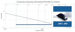
Element spacing is a key constraint when building a phased array. For the array to work as intended, designers need to ensure element spacing is at a half-wave or less. Wavelength decreases as frequency increases, so a common challenge in fully digital beamforming systems is ensuring that each path is spaced properly.
As mentioned above, reduced form-factor filters exist today and can address that problem. However, design becomes more challenging when posed with the task of including multiple filters, minimizing footprint, and maximizing performance in terms of selectivity and insertion loss. Knowles Precision Devices and Criteria Labs are experimenting with just that—most recently, the two companies have taken on the challenge of making a four-channel filter bank fit into sub-half-length space.
The Switched-Filter-Bank Packaging Solution
Beyond miniaturizing the filter components, switched filter banks continue to shrink with attention toward packaging. Attempting to push the boundaries on size while maintaining reliability, Knowles Precision Devices and Criteria Labs collaborated on a new concept. Depending on the size of the input and how narrow the output needs to be, a designer may opt for more channels.
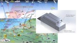
The concept is based on a four-channel filter bank. The design features a 3D-stacked structure, with an alternating pattern of filters and interposer boards, that mounts directly to the printed circuit board (Fig. 3). Minimizing internal spacing reduces the size of the filter bank to about 0.33 by 0.89 inches.
The 3D-stacked design focuses on element spacing by overcoming several challenges. Here, interposer boards have the ability to match signals and accommodate different dielectric constants. With signals above 10 GHz, any sort of mismatch—even a 50-Ω impedance mismatch—will cause them to degrade. Those signals must travel to and from the switched filter banks, and back down to the bottom of the board, without causing disruption to the signal or element spacing.
This design also integrates the switches directly into the filter bank to match performance every step of the way. The team ensures that every single interconnect has a matching circuit or construct to avoid disrupting the signal.
Through matching, 3D stacking, and integrated design, the switched filter bank is about 16X smaller than anything available. More importantly, it maintains RF performance, pulls the switches inside the package, and provides a surface-mount solution for lower-cost assembly (Fig. 4).
For EW and other specialized applications, filter banks often need a bit of customization to meet the requirements of a particular program. The task, whether you’re dealing with SWaP or fully digital beamforming, is to fit as much functionality as possible into a smaller space and maintain high performance.


