Measure Impedance And Insertion Loss In USB 3.0 Cables And Connectors
The very high bit rates employed by next-generation serial data standards extend well into the microwave region. For example, the upcoming highspeed Universal Serial Bus (USB3.0) supports transfer rates to 5 Gb/s over twisted-pair cables. Transmission of these high bit rates through connectors and cables results in considerable distortion because of channel dispersion. To keep this distortion to manageable levels, the standard specifies the impedance and return loss for mated cables and connectors. The latter measurement is represented by the S-parameter, S11. It must be normalized to the differential impedance of the cable, which is 90 Ohms.
While S-parameters are specified for measuring USB3.0 channels, the instrument of choice for measuring them is the time-domain reflectometer (TDR). TDR systems usually transmit a signal in the form of a voltage step into the device under test (DUT). Generally, they measure the reflected voltage as a function of time. Differential measurements are achieved by generating time-aligned voltage steps at opposite polarities. Differential signals are assumed in this article.
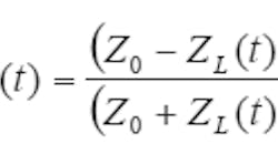
The reflected voltage is proportional to the impedance mismatch between the transmitter and the impedance of the DUT. This voltage is given by the following equation:
The impedance of the source is Z0 and that of the DUT is ZL(t). The reflection coefficient (t) is the ratio of the incident and reflected voltages Vr(t)/Vi(t). Although Equation 1 assumes that the source, cables, and connectors leading to the DUT are all matched, this is rarely the case. To compensate for imperfect cables and connectors, reference plane calibration is performed using calibrated open, short, and load (match) standards. Rearranging Equation 1 allows the impedance of the DUT to be measured as a function of time (or distance). As a result, one can directly measure the impedance using a properly calibrated TDR.
Figure 1 shows a plot of the impedance of a USB3.0 cable with mated connectors. The plot shows how the impedance varies as a function of time as the TDR step travels down the cable. Note the variation in the impedance at each end of the trace, which is due to the mated connector. According to the specification, this impedance variation must be within 13.5 Ohms of 90 Ohms when measured with a 50-ps (20 to 80 percent) rise time. The measurement rise time is important because the impedance variation is inversely proportional to the rise time of the TDR step. Because the specified rise time of the USB3.0 signal is 50 ps, matching this rise time in the measurement ensures that the impedance is "seen" by the signal.
Return loss or S11 is a frequency-domain measurement related to the reflection coefficient. The Fast Fourier Transform (FFT) of the normalized (through reference-plane calibration) reflection coefficient gives the return loss as a function of frequency. This measurement for the mated USB3.0 cable and connectors is shown in Figure 2. The horizontal scale is gigahertz per division, giving a range of DC to 20 GHz while the vertical scale is 10 dB per division. The return loss, which is approximately 15 dB to 2 GHz, becomes much smaller as the frequency increases. The finely spaced nulls in the response are caused by the connectors at each end of the cable. In contrast, the farther spaced nulls result from the impedance structure within the connector.
The return loss is referenced to the differential impedance of the TDR system, which is 100 Ohms. But the cable and connector impedance is 90 ohms as seen in Figure 1. This mismatch artificially reduces the return loss, as the USB3.0 transmitter differential impedance is 90 Ohms. To present the proper return loss, it is necessary to apply an impedance transformation to the measured S11. This transformation is given by the following relationships:
The conversion takes place in two steps. First, the complex load impedance must be computed from the complex S-parameter using the characteristic impedance of the measurement, which is 100 Ohms in this case. Next, the S-parameter will be computed from the load impedance using the new reference impedance of 90 Ohms. Because return loss is a function of frequency, this conversion is performed for each frequency.
For example, the complex return loss S11 = 0.53 - 0.12J measured in a 100-Ohm characteristic impedance converts to 90 Ohms:
The relations in Equation 2 were used to convert the insertion- loss measurement in Figure 2 to a 90-Ohm differential impedance. The two curves in Figure 3 show the return loss for 100- and 90-Ohm characteristic impedances.
The differential impedance of mated cable and connectors for the USB3.0 standard can be measured along with the insertion loss using a calibrated TDR system. Calibration is achieved by measuring open, short, and load standards at the reference plane, where the DUT is connected. Using a simple conversion, insertion loss can be used to compensate for the difference in impedance between the measurement system and the DUT.
REFERENCES
1. "Time Domain Spectrum Analyzer and "S" Parameter Vector Network Analyzer," James R. Andrews, Picosecond Pulse Labs application note AN-16a, November 2004.
2. "Converting S-parameters From 50-Ohm to 75-Ohm Impedance," Dallas Semiconductor/Maxim application note, Nov. 21, 2003.
