Quiet VCO Tunes 2.5-GHz WiMAX
This file type includes high resolution graphics and schematics when applicable.
Low-noise oscillators are essential for many communications systems, especially when they can maintain their low noise characteristics over wide frequency tuning ranges. As a boost for 2.5-GHz IEEE 802.16m WiMAX applications, a voltage-controlled oscillator (VCO) was developed with low phase noise—but also with low power consumption and in a small size.
One key to the excellent performance is noise filtering by means of a variable capacitor. The oscillator was implemented in a commercial semiconductor process from Taiwan Semiconductor Manufacturing Co. Ltd. (TSMC) to demonstrate its viability and performance. Both simulations and measured results indicate performance that should be quite attractive for 2.5-GHz IEEE 802.16m WiMAX use, with phase noise of -104 dBc/Hz offset 100 kHz from a 2.5-GHz carrier and -127.6 dBc/Hz offset 1 MHz from a 2.5-GHz carrier.
The WiMAX standard, IEEE 802.16, was developed to provide broadband wireless access for users over long distances.1 The original wireless standard has been amended by the WiMAX IEEE 802.16m standard with orthogonal-frequency-division-multiple-access (OFDMA) capability to provide an advanced air interface for operation in licensed bands. For WiMAX IEEE 802.16m applications, 2.5 GHz is an important frequency band.
The VCO is an important component building block in any wireless communications system, including for WiMAX applications, providing the local oscillator (LO) signals for RF/microwave mixers to facilitate upconversion and downconversion of signal frequencies in a system. Designers of VCOs face numerous challenges and goals, including achieving low phase noise, high linear VCO gain (KVCO), low power consumption, and low cost. Because of the poor noise performance of ring oscillators at frequencies above 1 GHz, inductive-capacitive (LC) VCO designs are widely used for frequencies above 1 GHz.
Recently, many LC VCOs were designed with goals to reduce phase noise. In one case, a low-phase-noise wide-tuning-range oscillator was based on resonant-mode switching. In this design, which switches between the two resonant modes of a high-order LC resonator consisting of two identical LC tanks coupled by capacitor and transformer, it was possible to achieve 3-dB less phase noise than for a VCO with single LC tank.2
In another design, researchers designed a resonant circuit with four p-n junction diode pairs, two spiral inductors, and a pMOS switch circuit, achieving a dramatic improvement in KVCO performance compared to a conventional oscillator.3 In addition, a novel resonant circuit consisting of transformer-based switched variable inductors and switched advanced-CMOS (A-MOS) varactor diodes was proposed to realize an ultrawide-tuning-range VCO4—in some cases, resulting in very low power consumption.5,6
Semiconductor VCOs developed for WiMAX applications often incorporate cross-coupled NMOS-PMOS device pairs and a top current source.7 This approach offers the advantages of low phase noise with a boost in the output amplitude and low 1/Δf3 noise.
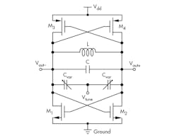
To achieve improved phase-noise performance, a proposed CMOS LC VCO design is shown in Fig. 1. It was designed without the top current source, and can achieve low phase noise while also maintaining low power consumption. The cross-coupled NMOS (M1, M2) and PMOS (M3, M4) transistor pairs generate negative impedance to compensate for the loss of the LC tank, as described in Eq. 1:
where Zin is the input impedance, gmn is the transconductance of the NMOS device, and gmp is the transconductance of the PMOS device. PMOS technology offers the means of suppressing flicker noise and controlling current consumption. The VCO resonator consists of an inductor (L), fixed capacitor, and A-MOS variable capacitance. The A-MOS technology was chosen with the intent of increasing the VCO tuning range.
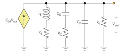
According to an equivalent circuit of the VCO (Fig. 2), conditions for oscillation can be described by Eqs. 2 and 3:
where:
LB = the VCO inductor;
CD = a fixed capacitor;
Cvar = a variable capacitor;
CP = the parasitic capacitance;
R = the resistance of the circuit;
QB = the quality factor (Q) of the inductor; and
QC = the Q of the capacitor.
Part of the design challenge is to establish the required gm values for the NMOS and PMOS devices by appropriate adjustment of the device weight-to-length (W/L) ratios. Oscillator phase noise depends a great deal on the Q of the tank circuit used for a particular oscillator. As a result, improved phase noise requires careful attention to the tank circuit.
This file type includes high resolution graphics and schematics when applicable.
A Closer Look
This file type includes high resolution graphics and schematics when applicable.
A VCO’s phase noise stems from passive components and MOS active devices in the oscillator circuit; VCO phase noise, of course, can impact the sensitivity of an RF/microwave receiver. Leeson’s equation has often been used to analyze and optimize the phase-noise performance of VCOs and other oscillators, and its expression can be shown by means of Eq. 4:
where:
Q = the quality factor;
F = the noise factor;
k = Boltzmann’s constant;
T = the thermodynamic temperature;
Psig = the signal power produced by the VCO;
w0 = the oscillation frequency of the VCO;
Δw = the frequency offset; and
Δw1/f3 = the inflection frequency between 1/f3 and 1/f2.
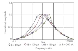
According to Leeson’s equation, a high Q yields low phase noise. Figure 3 offers simulated Q values for different sizes of standard and symmetric-mode octagonal inductors at 2.5 GHz. An inductor with high Q was chosen for the 2.5-GHz VCO to achieve low phase noise.
Third-order and higher-order harmonic signals from the LC resonator are at low levels that can be considered negligible; the even harmonics flow in a common-mode path through the active devices in the VCO circuit. Because of this, the effects of the second-harmonic signals, which contribute to oscillator phase noise, must be taken into account. A traditional method of filtering involves placing a large-valued shunt capacitance parallel to the grounded MOS devices. But if this large value for the shunt capacitor is not carefully chosen, it can lead to self-modulation effects.
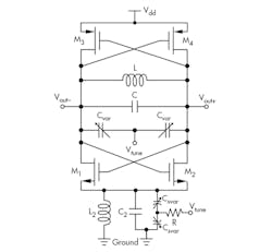
To avoid problems with self-modulation effects while also providing low phase noise, the filtering technique used for the proposed VCO involved an inductor and variable capacitors. Figure 4 shows the proposed VCO and the filtering technique. The capacitance value of the variable capacitors (Cvar can be set to an appropriate value when the oscillation frequency is changed. To maintain high Q for the resonator, L2 = L1 and C1 + Cvar/2 = 4(C2 + Cvar/2).
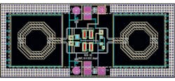
The proposed VCO schematic and layout was designed and simulated with Cadence Spectre SPICE-based circuit simulator from Cadence Design Systems and fabricated with TSMC’s 0.18-μm 1P6M silicon CMOS process for use with a +1.6-VDC voltage supply. Figure 5 shows the final physical layout of the VCO, with a core integrated-circuit (IC) layout size of 997.8 × 337.6 μm2.
Figure 6 displays post-layout-simulation results (the dashed curve) for the VCO’s frequency tuning range and for the VCO gain, KVCO (the curve denoted by x), with a frequency tuning range of 2.4 to 2.6 GHz. Ideally, KVCO should remain constant throughout the frequency tuning range of the VCO, although these simulations show that the value of KVCO for this proposed VCO design varies somewhat (from 0.1 to 0.2) across the tuning range. This is due to the fact that the A-MOS variable capacitor is not strictly linear in its changes of capacitance with voltage, resulting in nonlinear variations in the VCO’s tuning characteristics.
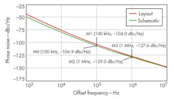
Figure 7 shows the phase noise of the VCO for the schematic-circuit and post-layout simulations. The post-layout simulation predicts phase noise of -104 dBc/Hz offset 100 kHz from a 2.5-GHz carrier and -127.6 dBc/Hz offset 1 MHz from the same carrier (the dashed curve). Parasitic circuit elements will degrade the phase-noise performance of the LC VCO, so the circuit layout should be carefully designed and implemented to minimize parasitic elements. A DC simulation of the circuit design indicates that the core power consumption of the VCO is 8.24 mW from a +1.6-VDC voltage supply.
To characterize and compare the performance of the proposed VCO with previously published oscillators, a widely used figure of merit (FOM)7-11 as described in Eq. 5 was applied:
where:
L(Δf) = the VCO phase noise;
Δf = the offset frequency;
f0 = the carrier frequency; and
PDC = the DC power consumption of the VCO.
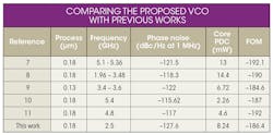
According to Eq. 5, the FOM phase noise for the proposed VCO design is -186.4 dBc/Hz. The table offers a comparison of the proposed VCO to different VCO designs from recent years. The phase noise of the proposed VCO is lower than values from numerous published reports7-11 while, at the same time, operating with lower power consumption, better FOM, and small semiconductor chip area.
Based on TSMC’s 0.18-μm CMOS process, the VCO draws only 8.24 mW power from a +1.6-VDC supply with a layout measuring 997.8 × 337.6 μm2. It offers many of the characteristics well suited for WiMAX IEEE 802.16m applications.
Wei Wang, Professor
Yao Liang, Master’s Student
Chen Zhao, Master’s Student
Wenqi Cai, Master’s Student
Xiao Mo, Master’s Student
Jun Yuan, Associate Professor
Guanyu Wang, Associate Professor
College of Electronics Engineering, Chongqing University of Posts and Telecommunications, Chongqing 400065, People’s Republic of China
This file type includes high resolution graphics and schematics when applicable.
References
This file type includes high resolution graphics and schematics when applicable.
1. B. Li, Y. Qin, C.P. Low, and C.L. Gwee, “A survey on mobile WiMAX [wireless broadband access],” IEEE Communications Magazine, Vol. 45, No. 12, 2007, pp. 70-75.
2. G. Li, L. Liu, Y. Tang, and E. Afshari, “A low-phase-noise wide-tuning-range oscillator based on resonant mode switching,” IEEE Journal of Solid-State Circuits, Vol. 47, No. 6, 2012, pp. 1295-1308.
3. S. Kurachi, T. Yoshimasu, L.I.U. Haiwen, and K. Yonemura, “A SiGe BiCMOS VCO IC with highly linear KVCO for 5-GHz-band wireless LANs,” IEICE Transactions on Electronics, Vol. 90, No. 6, 2007, pp. 1228-1233.
4. L.I.U. Qing, Y. Takigawa, S. Kurachi, and T. Yoshimasu, “A 1.2-3.2 GHz CMOS VCO IC Utilizing Transformer-Based Variable Inductors and AMOS Varactors,” IEICE Transactions on Fundamentals of Electronics, Communications, and Computer Sciences, Vol. 94, No. 2, 2011, pp. 568-573.
5. M. Locher, J. Kuenen, and A. Daanen, “A versatile, low power, high performance BiCMOS MIMO/diversity direct conversion transceiver IC for WiBro/WiMAX (802.16 e),” IEEE Journal of Solid-State Circuits, Vol. 43, No. 8, 2008, pp. 1731-1740.
6. A. Mazzanti and P. Andreani, “A Push-Pull Class-C CMOS VCO,” IEEE Journal of Solid-State Circuits, Vol. 48, No. 3, 2013, pp. 724-732.
7. K.C. Kuo and C.W. Wu, “A low phase noise VCO for 5-GHz WiMAX/WLAN frequency synthesizer,” in IEEE International Electron Devices and Solid-State Circuits Conference (EDSSC), 2013, pp. 1-2.
8. W. Zou, X. Chen, K. Dai, and X. Zou, “Switched-inductor VCO based on tapped vertical solenoid inductors,” IET Electronics Letters, Vol. 48, No. 9, 2012, pp. 509-511.
9. X. Hu, F. Huang, T. Li, and X. Tang, “A wide band 0.13-μm CMOS LC-VCO for IMT-advanced and UWB applications,” Journal of Semiconductors, Vol. 34, No. 1, 2013, pp. 015004-6.
10. M.T. Hsu, Y.T. Hsu, and Y.Y. Lee, “Low power and low phase noise CMOS VCO based on cross-coupled topology with capacitor filter,” in IEEE Asia Pacific Microwave Conference (APMC), 2013, pp. 328-330.
11. J. Jian and F. Xiangning, “A fully integrated LC VCO with 1V voltage supply for wireless sensor network applications,” in IEEE Advanced Technologies for Communications Conference (ATC), 2013, pp. 469-472.
This file type includes high resolution graphics and schematics when applicable.


