This file type includes high resolution graphics and schematics when applicable.
Modern receivers often use high-speed analog-to-digital converters (ADC) to sample signals at intermediate frequencies (IFs) or even at radio frequencies (RFs), such as software-defined radios (SDR) receivers.1 However, the amplitude of an incoming signal may exceed an ADC’s maximum permissible input level during large-signal conditions. To avoid damaging or degrading the ADC, amplitude limiting is necessary. While automatic-gain-control (AGC) circuitry can be effective for controlling IF amplitude excursion in traditional single-carrier systems, it is not desirable in modern multicarrier applications.2
One solution is to cap the IF amplitude excursion with a limiter. Unfortunately, a new problem is then created: The strong nonlinearity that is required of a good limiter also makes it an efficient generator of harmonics. The lower-order harmonics, especially second-harmonic signals, are particularly troublesome because they can fall inside the passband of a wideband ADC. ADC protection based on clamping with positive-negative (PN) or Schottky diodes are less linear than limiting with PIN diodes.
To minimize second-harmonic production in a PIN diode limiter, the authors investigated several circuit configurations and also diode intrinsic-layer heights. The experimental results of those investigations, along with some proposed solutions and their tradeoffs, are presented here.
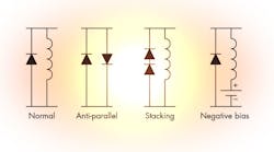
A number of different limiter circuit configurations are commonly used for protection purposes. The classic self-biased limiter configuration comprises a diode and a choke shunting a transmission line.3 The choke serves as the DC return in the diode’s RF detector role. In the absence of a signal, the choke also discharges the charge stored in the diode and the DC blocking capacitors (Fig. 1).
Under small-signal conditions—i.e., below the limiting threshold—the rectified current is insufficient to lower the diode junction resistance. As a result, the diode appears as a capacitance shunted by a large resistance. The diode can be characterized by a dielectric relaxation frequency (fDR), which is given by:
fDR = 0.5πρε
where:
ρ = the intrinsic (I) layer bulk resistivity and
ε = 1 × 10-12 F/cm
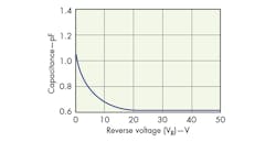
This capacitance varies inversely with the applied voltage (Fig. 2). An RF voltage can modulate this junction capacitance to produce distortion through the varactor effect. Since capacitive reactance decreases with increasing frequency, the distortion becomes worse with increasing frequency—i.e., in the opposite direction to the forward-biased condition.4
Another diode limiter configuration, the anti-parallel configuration, is the basis of the bidirectional clamp5,6 and the subharmonic mixer7, both of which use Schottky diodes. Since the even-order distortion generated by each diode will have opposite polarities, self-cancellation will occur to the extent that the diodes are matched. An anti-parallel configuration can be adapted with PIN diodes to reduce limiter distortion, with a bonus feature of the anti-parallel configuration being that it doesn’t need a choke for the DC return.
A third diode limiter configuration—the stacked configuration—reduces the overall capacitance, because the two diodes are connected in series. An alternative explanation is that the voltage across each diode is halved compared to a single diode. Stacking has been successfully used to reduce distortion in field-effect-transistor (FET) attenuators. Yet it remains to be seen if diode stacking can improve limiter linearity.
Reverse-bias (Vr) techniques have been shown to reduce distortion in PIN diode switches,4 and the mechanism is attributed to the negative bias preventing RF rectification.10 Reverse-bias techniques also widen the diode’s depletion zone. It is conceivable that the reduced junction capacitance is partly responsible for the improvement in linearity. Determining whether this method is the optimum means of reducing limiter distortion is a matter of sizing up the different diode limiter approaches.
Self-biased limiters typically use very thin PIN diodes in the 1-to-7 μm range11 because of their low turn-on thresholds. The 1.5-μm PIN diode,12 which forms the bulk of this work, has about a +10-dBm threshold.13 But the thin diode’s current-voltage (C-V) profile, which changes very abruptly around 0 VDC (Fig. 2), increases its susceptibility to varactor modulation.
On the other hand, thick diodes (e.g., 22.5 μm), have much flatter C-V profiles and, thus, should be less susceptible to the varactor effect. But a 22.5-μm diode requires more current to turn on than a thinner diode. Therefore, it will have an unusably high limiting threshold.
This file type includes high resolution graphics and schematics when applicable.
A Closer Look
This file type includes high resolution graphics and schematics when applicable.
The limiter detailed in this article is intended for protecting an ADC with a 1-GHz bandwidth. Hence, only signal frequencies below 500 MHz are of concern because the harmonics of higher frequencies will fall outside of the ADC passband. This ADC overloads when its input exceeds 0.7 V RMS, which corresponds to +10 dBm in a 50-Ω environment. The limiter’s harmonic level will be measured at this signal level because it represents worst-case conditions.
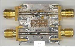
Candidate diode limiter solutions were assembled on printed-circuit boards (PCBs) of a common design (Fig. 3). The 50-Ω coplanar-waveguide-with-ground (CPWG) transmission lines were etched on one side of 30-mil-thick FR-4 PCB, while the opposite side of the circuit material serves as the ground plane. The measurement reference planes were where circuit board’s SMA connectors interface with the coaxial cables that link the test board’s signals to the test equipment.
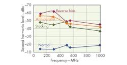
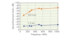
Modification of a standard limiter circuit can reduce distortion by 18 to 30 dB. Below 500 MHz, more than 30 dB improvement can be achieved (Fig. 4). The greatest improvement was seen in the reverse-biased limiter (with Vr = 1 V), followed by the anti-parallel configuration and then the stacked configuration. The harmonic distortion levels of these three candidate solutions become worse at higher frequencies in accordance with the theory of unbiased PIN diodes.
On the other hand, the distortion in the normal limiter diode configuration exhibits the opposite trend of improving with frequency—i.e., this configuration’s turn-on threshold is equal to the test signal and therefore its diode is forward-biased.
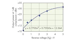
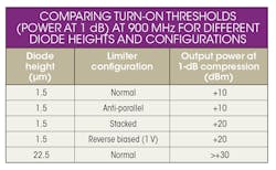
Even though harmonic suppression increases with the reverse voltage magnitude, values higher than 1 V are not viable because the threshold is increased exponentially (Fig. 5). Since the diode capacitance changes very little between 0 and 1 V (Fig. 2), the distortion improvement is more likely due to the reverse bias preventing RF rectification. Stacking also raises the original about +10 dBm threshold to about +20 dBm. Of all the evaluated solutions, only the anti-parallel arrangement does not increase the limiting threshold.
A thicker PIN diode can also reduce limiter distortion. Replacing the original 1.5 μm thick diode with a 22.5 μm diode14 lowers the second harmonic distortion by 40 to 60 dB in the evaluated frequency range (Fig. 6). The thick diode’s distortion reduces with frequency before levelling off above about 500 MHz; this inflection point coincides with the dielectric relaxation frequency (fDR).
As predicted earlier, the 22.5-μm diode limiter has an unusably high limiting threshold of >30 dBm (see table). One possible way to achieve a more reasonable threshold with the 22.5-μm diode is to utilize it in a quasi-active DC driven limiter.15 Instead of depending on RF rectification for the bias current, the quasi-active DC driven limiter sources the current through a DC amplifier (Fig. 7). Thereafter, the limiting threshold can be varied by changing the DC amplifier’s gain.
On the downside, this configuration incurs much more space and cost than the self-biased limiter. Alternatively, if the ADC has an overflow indicator output, it can be used to drive the DC amplifier directly, thus saving on a detector and a coupler.
To evaluate the harmonic levels of these different diode limiter candidates, a special test setup was assembled with the capability of measuring low-level signals (Fig. 8). Most commercial signal generators offer second-harmonic levels of around -30 dBc. Since almost all of the limiters being evaluated would produce harmonic signal levels of less than the test signal generator being used in the experiments (a model 83712B from Hewlett-Packard Co.), lowpass filters were required to clean up the test signals.
Different lowpass filters were needed for each test frequency. An attenuator pad at the input of the device under test (DUT) buffers against mismatches when a limiter is turned on (ideally, an isolator could be used if available for each test frequency). To present the spectrum analyzer in the test setup from being overdriven, its attenuator is set to a relatively large large (30 to 40 dB). To verify that the test setup’s residual harmonic level is lower than that of a DUT, the DUT is initially replaced by the “THRU” connection when making measurements.
The low-distortion limiter required by wideband ADCs can be realized by modifying either the circuit configuration or the diodes’ physical attribute. Stacking, anti-paralleling, and reverse-biasing of limiter circuits can reduce the second-harmonic amplitude by tens of decibels over conventional limiter configurations. Selecting a thicker diode can also significantly reduce distortion, but this requires additional circuits to enable limiting at reasonable input-power levels.
With the exception of the anti-parallel configuration, all the other solutions suffer from higher turn-on threshold voltages. Hence, the latter approach is the most cost-effective solution.
Acknowledgment
The author wishes to thank Raymond W. Waugh for designing the test PCB.
Chin Leong Lim, Engineer
Avago Technologies, Penang, Malaysia
This file type includes high resolution graphics and schematics when applicable.
References
This file type includes high resolution graphics and schematics when applicable.
1. P. Cruz, N.B. Carvalho, and K.A. Remley, “Designing and testing software-defined radios,” IEEE Microwave Magazine, June 2010, pp. 83-94.
2. B. Brannon and B. Schofield, “Multicarrier WCDMA Feasibility,” Analog Devices, Application Note AN-807, 2006, www.analog.com.
3. K.C. Kupta, “Microwave Control Circuits,” in Microwave Solid-State Circuit Design, 2nd ed., I. Bahl and P. Bhartia, Eds., Wiley, Hoboken, NJ, 2003, pp. 682-683.
4. R.H. Caverly and G. Hiller, “Distortion in Microwave and RF Switches by Reverse Biased PIN Diodes,” 1989 MTT-S International Microwave Symposium Digest, pp. 1073-1076.
5. R.W. Waugh, “Schottky diodes solve digital circuit problems,” Hewlett-Packard Co., design tip, January 1999.
6. Avago Technologies, application note, “Non-RF applications for the surface mount Schottky diode pairs HSMS-2802 and HSMS-2822.”
7. M.V. Schneider Jr. and W.W. Snell, “Harmonically Pumped Stripline Down-Converter,” MTT-S Transactions of Theory & Techniques, Vol. MTT-23, No. 3, March 1975, pp. 271-275.
8. D.R.Webster, M.T. Hutabarat, D.G.Haigh, and A.E.Parker, “Designing Low Distortion Continuously Variable Attenuators for Microwave Frequencies,” IEE Coloquium on Low Power IC Design, January 2001.
9. M. Granger-Jones, B. Nelson, and E. Franzwa, “A broadband high dynamic range voltage controlled attenuator MMIC with IIP3> +47dBm over entire 30-dB analog control range,” Proceedings of the 2011 IEEE Microwave Symosium, 2011.
10. L. Drozdovskaia, “Frequency properties of a reverse biased thick switching PIN diode,” Applied Microwave & Wireless, February 2002, pp. 106-114.
11. Skyworks Solutions, datasheet, “Limiter diodes.”
12. Avago Technologies, product specification, “HSMP-382x series and HSMP-482x series.”
13. Avago Technologies, application note 1050, “Low cost surface mount power limiters,” 1999.
14. Avago Technologies, product specification, “HSMP-386x series.”
15. Alpha Industries, application note 80300, “Characteristics of semiconductor limiter diodes.”
This file type includes high resolution graphics and schematics when applicable.
