This file type includes high resolution graphics and schematics when applicable.
Low-noise amplifiers (LNAs) form the input stage of the receiving part of nearly any communications system. The main task of these subcircuits is to amplify the wanted signal without deteriorating the signal-to-noise ratio. In most cases, the desired signal is very weak. The noise figure is seen as the main describing figure of merit for the transistors used in such applications. It determines the minimum amount of noise that is added in the transistor stage. The noise figure is not a hard figure, as it depends on the bias and especially the input matching conditions.
According to many microwave textbooks, nothing is easier than the design of a matching network for a specific transistor. The engineer simply needs to know the S-and noise parameters at an appropriate bias point for that transistor. Yet a design problem might arise if stability is a concern. The noise match is routinely done by setting the input noise and output gain match, which is a standard procedure in many textbooks (e.g., Ref. 1, Ch. 4.1.2). There is not much room to influence or even improve the stability factor. As a result, stability is often checked only after the design is completed.
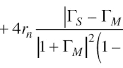
The "traditional" way of making a noise match is repeated here. For a given transistor, a set of S-and noise parameters, Snm and N, is available at the bias point of interest. The noise match, τM, is taken from the set of noise parameters, N, at the operating frequency. The load match, τL (index L means Load), is then calculated for maximum gain. With this procedure, the question of stability is ignored. It can only be checked after the τL is determined. With a general τS (index S means Source, presented to the input of the transistor), the noise figure, F, is calculated as:
where rn = Rn/Z0. Note that Z0 is the characteristic impedance of the transistor (in most cases, 50 Ω). Two points should be emphasized at this stage:
- As can be seen from Eq. 1, only the input impedance τS determines the noise figure, F, from an application point of view. FMIN, rn, and τM are characteristics of the transistor in the selected bias point. To get the minimum noise figure available, FMIN, τS should be set to TM.
- F is not affected by the load impedance, τL
The stability of a given transistor is mostly described by the K-factor, which is computed as follows:
Because many textbooks explain why K > 1 means unconditional stability, that information is not repeated here (see Ref. 2 or Ref. 3 for further explanation). With the procedure described, it is helpful if the transistor is unconditionally stable at any frequency. Unfortunately, this is not the case for many devices. In a lot of applications, the circuit designer is choosing the transistor according to parameters presented on its datasheet, such as available gain, third-order intercept point (IP3), operating voltage, FMIN, and others. The last step is to check the transistor's Sparameters for stability. In the design stage, it may be found that the transistor tends to oscillation. This knowledge is especially damaging when gained at the production stage.
Fortunately, it is possible to " stabilize" a transistor when the LNA is designed. The overall rule is to decrease the gain of the entire LNA. This approach will help to increase the K-factor and thus stabilize the LNA. From a circuitdesign point of view, the following possibilities exist:
- Mismatch the output. This approach will decrease the stage's gain and improve the stability. But it also may lead to matching problems regarding the following LNA stage. In addition, S22 may be deteriorated. Looking at the numerator of Eq. 2, it is clear that this approach may not really help to increase the K-factor.
- Introduce some amount of resistive feedback. In a common emitter/source circuit, feedback is applied between the base/gate and collector/drain. In most cases, a capacitor also will be needed to block the different DC levels from each other. Because this method also is changing the input parameters, significant changes in the noise parameters need some modifications.
- Load the output (collector/drain) resistively to ground. Many advantages come with this technique. The gain is reduced for some amount and S22 is improved if the resistive loading is made in a proper region. These two effects work in a common direction to improve the K-factor. In addition, this technique can be easily incorporated in the output biasing circuit.
The starting point of the last technique is an s2p-file of a model NE661M04 transistor from NEC/ California Eastern Laboratories (www.cel.com) in Touchstone file format including the noise parameters. The device for this example is a silicon-bipolar transistor that provides unconditional stability in the LNA design that is presented.
To design the LNA, the target specifications must first be defined. Because this example should show the stabilizing part of the design phase, only the small-signal, linear specifications are given here:
- Frequency: 2 GHz (narrowband design)
- Gain (S21): >16 dB
- Noise figure:
- Stability: unconditionally stable (K>1 for all frequencies)
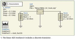
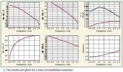
Compared to the design center frequency, an initial check of the S-parameters in the first step shows that the Kfactor remains less than unity at higher frequencies. In this case, the transistor would remain unstable with the normal procedure by just setting a noise match at the input and a gain match at the output. The ADS linear testbench and data display are shown in Fig. 1 and Fig. 2, respectively.
In the data display, the four S-parameters are given versus the frequency accompanied by the noise figure and K-factor (lower right display). The K-factor stays below unity through approximately 2.5 GHz and therefore also at the intended operating frequency at 2 GHz. The transistor's behavior is potentially unstable.
Such behavior may lead to problems in the LNA. If this LNA is the first amplifier in the signal chain connected to the antenna, its input impedance may be affected by the load imposed by the antenna. Such effects as tuning or degrading the antenna by touching small mobile phones with the user's hand or snow on an LNB horn may affect the LNA's source impedance. Of course, the impedance can be checked with the method of stability circles. If the LNA is not unconditionally stable at all frequencies, however, these ambient interactions will not just degrade the noise figure. They also can start transistor oscillations that may shift the bias point ( mostly to higher current consumption) or even destroy the transistor. Checking the stability of an LNA is thus a kind of quality issue for the entire product.
Page Title
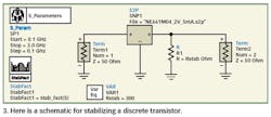
In the second step, the transistor will be stabilized. As stated previously, this stabilization will be done with a resistor that shunts the output (the collector or drain of the transistor used) to ground. The resistor's value is then tuned and checked to see if it reached unity of the K-factor. The change in the linear parametersespecially S22 and S21will improve so that the K-factor increases. Because this method is always a trade-off, it should be considered carefully.
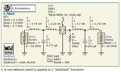
The ADS schematic for the LNA circuit is shown in Fig. 3.
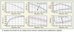
The simulation results that are displayed when tuning the output shunt resistor are presented in Fig. 4.
Some influences can be observed as the shunt resistor, Rstab, is decreased. The curves in this display are starting with Rstab set on infinity (red line: same results as before) and then set to 600 Ω stepped down to 100 Ω in 100-Ω steps.
The gain (S21) is decreasing as the stabilizing resistor is decreased. In contrast, the K-factor is increasing significantly. Note that the gain must not be reduced enough to put the K-factor in a "safe" area beyond unity. The output return loss also is affected because the shunt resistor is applied at the output. As an Rstab of 300 Ω is applied at the output, the gain (S21) is decreased by about 0.5 dB from 17.2 to 16.7 dB.
With this resistor, the K-factor is increased to a safe figure beyond unity for all frequencies. The transistor behaves in an unconditionally stable manner with this application. The noise figure is only slightly affected (within a tenth of a dB). These changes can therefore be ignored. In addition, S11 is almost completely unaffected.
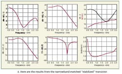
For the third step, the design is completed with the "new S-parameters" including Rstab. Rstab is incorporated into the transistor's S-parameters. It can be seen as a new set of S-parameters. A narrowband, lumped-element, input-noise and gain match on the output is performed at the operating frequency (Figs. 5 and 6).
The match is carried out as if it was done without any modification. First, the load impedance is calculated (from the resulting S-parameters with "stabilization" and the given source load from the noise parameters). The impedances are then carried out with the help of lumped elements.
The values of the capacitors and inductances are quite odd. The results from the exact mathematics must therefore be modeled with real models for the passive components. To get some benefit from the simulation, the capacitors in particular must be modeled with a series capacitor inductance. The fourth design step follows, although that step is omitted here. The major point to be emphasized is that the Kfactor is raised with the technique that was previously explained. This technique also is applicable to other transistors and different specifications.
Practical Considerations
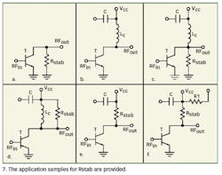
There are different ways to implement the stabilizing resistor, Rstab, shown in Fig. 7a. In the following explanations, note that the matching circuits at input and output are omitted for clarity. The capacitors at input and output, which are used for DC-cutoff to the preceding and following stages, also are not shown. Even if a bipolar transistor is shown in the application examples, keep in mind that these examples also work with FETs.
The most common biasing method is to apply an inductor from the device's RF output port to the DC source shunted by a capacitor (Fig. 7b). The main question is how to incorporate the stabilizing resistor, Rstab. (Fig. 7c)shows a direct implementation of Rstab. Because the resistor is galvanically set to ground, it works as simulated down to DC. The disadvantage is that an additional DC current, I=Vcc/Rstab, is drawn from the supply. When the entire system is not powered from batteries, however, this issue may not be a major problem.
The implementation in (Fig. 7d) shows reverse consideration toward (Fig. 7c.) Here, Rstab does not provide any DC-current distribution. Its frequency response is determined by the capacitor, C. Because the DC supply is usually shunted with high-value capacitors (up to the F range), this determination is not really a problem. If the supply voltage shows the right level to bias the transistor directly, this configuration seems to be the most advantageous one. Note that Rstab is shorted by the biasing inductor, Lc. It could therefore be neglected in terms of DC.
If the supply voltage is somewhat too high, the configurations in (Fig. 7e)and (Fig. 7f) come into play. Rstab is used to drop some voltage with it. Once the collector (drain) current is fixed, the voltage drop can be calculated. If the collector (drain) current can be set so the required voltage drop can be done with Rstab, the configuration looks like (Fig. 7e). If a higher voltage drop is required, the needed overall resistor value can be split up between Rstab and R1. Note that a capacitor is needed between the resistors to make Rstab effective in terms of RF.
This file type includes high resolution graphics and schematics when applicable.
