This file type includes high resolution graphics and schematics when applicable.
Oscillators are critical components in RF and digital designs. Although oscillator circuitry may already be provided as part of an integrated circuit (IC), a product-design engineer may still be required to select the crystal resonator and external capacitors. To achieve final product success, it is important that the designer has a basic understanding of how an oscillator and crystal function to select the correct crystal and external capacitors for the device. Poor crystal selection can lead to a product that does not operate properly, fails prematurely, or will not operate over the intended voltage and temperature range. What follows is a basic explanation of crystal resonators and crystal oscillators. Armed with this basic knowledge, a product design engineer will have the insight to select the correct crystal and external capacitors for an IC. Designers will also obtain an understanding of the interrelationships of the various circuits available that make up an oscillator circuit and what to consider when working with RF ICs and commercially available microcontrollers.
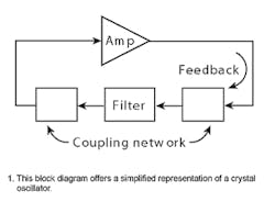
Reduced to its simplest components, a crystal oscillator consists of an amplifier and a filter operating in a positive feedback loop (Fig. 1).
To begin oscillation, the circuit must satisfy the following Barkhausen criteria: 1) the loop gain exceeds unity at the resonant frequency, and 2) the phase shift around the loop is n2π radians (where n is an integer. Intuitively, it can be seen that the amplifier provides the gain for the first criteria. The amplifier is inverting, causing a π rad (180-deg.) phase shift to meet the requirements of the second criterion. The filter block provides an additional π rad phase shift for a total of 2-π rad (360 deg.) around the entire loop. By design, the filter block inherently provides the phase shift in addition to providing a coupling network to and from the amplifier. The filter block also sets the frequency of oscillation, using a tuned circuit (inductor and capacitor) or crystal.
Operation of an oscillator is generally broken up into two phases: startup and steady-state operation. An oscillator must start itself with no external stimulus. When the power is first applied, voltage changes in the bias network result in voltage changes in the filter network. These voltage changes excite the natural frequency of the filter network and signal buildup begins and the signal developed in the filter network is small. Positive feedback and excess gain in the amplifier continuously increases the signal until the nonlinearity of the amplifier limits the loop gain to unity. At this point, the oscillator enters steady-state operation; the time from power on to steady-state operation is the oscillator start-up time.
An oscillator's steady-state operation is governed by the amplifier and the tuned circuit of the filter block. Loop gain steadies at unity due to the non-linearity of the amplifier. The tuned circuit reactance will adjust itself to match the Barkhausen phase requirement of 2-π rads. During steady-state operation, the main concerns are the power output and loading of the tuned circuit. The amplifier circuit is typically implemented with a bipolar junction transistor (BJT) or metal-oxide-semiconductor field-effect transistor (MOSFET). The linear characteristics of the transistor determine the starting conditions of the oscillation while the nonlinear characteristics determine an oscillator's operating point.
The filter block sets the frequency that the oscillator will operate, which is accomplished by using an inductive-capacitive (LC) tuned circuit or crystal.
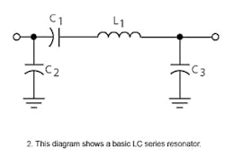
Figure 2 depicts a basic shunt-C coupled LC-series resonator that provides phase shift and a coupling network. Since an inverting amplifier is being used, the filter block must provide a µ-rad (180-deg.) phase shift to satisfy the second Barkhausen criteria. There is an unlimited number of circuit combinations for oscillators. Numerous circuits take on the name of their inventors (i.e., Butler, Clapp, Colpitts, Hartley, Meacham, Miller, Seiler, and Pierce) and, in turn, many of these circuits are derivatives of one another. Readers should not worry about a particular oscillator's nomenclature, but should focus on operating principles.1 No one circuit is universally suitable for all applications2 and the choice of oscillator circuit depends on device requirements.
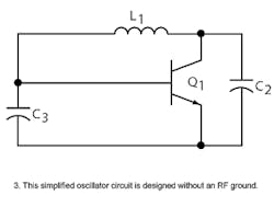
The next step in developing a crystal oscillator is to add circuitry to the simplified oscillator block diagram shown in Fig. 1. Figure 3 shows a simplified oscillator circuit drawn with only the RF components, no biasing resistors, and no ground connection.
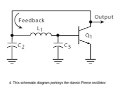
The inverting amplifier is implemented with a single transistor and the feedback mechanism depends upon which ground reference is chosen. Of the numerous oscillator types, the three most common ones are Pierce, Colpitts, and Clapp configurations, and each consists of common circuitry except that the RF ground points are at different locations. The type of oscillator commonly employed in ICs is the Pierce configuration (Fig. 4).
It has many desirable characteristics, including the capability of operating over a wide range of frequencies with very good short-term stability.3 Although inductors and capacitors are convenient for use in oscillator-tuned circuits, the primary disadvantage of this type of oscillator is the tendency to drift with changes in temperature, power-supply voltage, or mechanical vibrations. Setting the frequency of an LC oscillator requires precise manual tuning.
Understanding Quartz
An understanding of how a quartz-crystal resonator works can provide design engineers with a better understanding of crystal oscillators. Quartz crystals have very desirable characteristics for use in tuned oscillator circuits, since their natural oscillation frequencies are very stable. In addition, the resonance has a very-high quality factor (Q), ranging from 10,000 to several hundred thousand. In some cases, Q values of two million are possible. Ultimately, however, Q values and stability are the principle limitations of crystal-based oscillators.
The practical frequency range for fundamental-mode AT-cut quartz crystals is 600 kHz to 30 MHz. Crystals for fundamental frequencies higher than 30 to 40 MHz are very thin and fragile. Crystals are used at higher frequencies by operation at overtones of the fundamental frequency. Ninth-overtone crystals are used up to approximately 200 MHz, the practical upper limit of crystal oscillators. This article will limit its discussion to the use of fundamental-mode crystals.
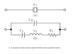
Quartz is a piezoelectric material and when an electric field is placed upon it, a physical displacement occurs. Interestingly, an equivalent electrical circuit can be written to represent the mechanical properties of the crystal. The schematic symbol for a quartz crystal is shown in Fig. 5a and the equivalent circuit for a quartz crystal near fundamental resonance is shown in Fig. 5b.
The equivalent circuit is an electrical representation of the quartz crystal's mechanical and electrical behavior and it does not represent actual circuit components. The crystal is, after all, a vibrating piece of quartz. The circuit elements C1, L1, and R1 are known as the motional arm and represent the mechanical behavior of the crystal element, while capacitor C0 represents the electrical behavior of the crystal element and holder.
The equivalent circuit in Fig. 5b represents one oscillation mode. For the types of crystal oscillators related to this article, the focus will remain on fundamental-mode crystals. A more complex model can represent a crystal through as many overtones as desired. For the sake of simplicity, this simple model is usually employed and different values are used to model fundamental or overtone modes. Spurious resonances occur at frequencies near the desired resonance. In a high-quality crystal, the motional resistance of spurious modes is at least two or three times the primary resonance resistance and the spurious modes may be ignored. In this model, C1 represents motional arm capacitance (in Farads). It represents the elasticity of the quartz, the area of the electrodes on the face, and the thickness and shape of the quartz wafer. Values of C1 are in the range of femtofarads (10−15 F or 10−3 pF).
L1 represents motional arm inductance (in Henrys). It represents the vibrating mechanical mass of the quartz in motion. Low-frequency crystals have thicker and larger quartz wafers and range in a few Henrys. High-frequency crystals have thinner and smaller quartz wafers and range in a few megaHenrys. R1 is the resistance (in Ω). It represents the real resistive losses within the crystal. Values range from 10 Ω for 20-MHz crystals to 200 kΩfor 1-kHz crystals. C0 is the shunt capacitance (in Farads). It is the sum of capacitance due to the electrodes on the crystal plate plus stray capacitances due to the crystal holder and enclosure. Values of range from 3 to 7 pF.
Electrical specifications
In selecting a crystal, a designer should be familiar with the electrical specifications found in a data sheet or catalog (Table 1).
When purchasing a crystal, the designer specifies a particular frequency, along with load capacitance and mode of operation. Notice that shunt capacitance C0 is typically listed as a maximum value and not as an absolute value. Notice also that motional parameters C1, L1, and R1 are not typically provided in the crystal data sheet. They can generally be obtained from a crystal manufacturer, or from measurements. Table 2 shows equivalent-circuit values for an example crystal.
In Table 2, shunt capacitance is provided as an absolute value. However, shunt capacitance can be measured with a capacitance meter at a frequency much less than the fundamental frequency.
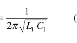
A crystal has two resonant frequencies characterized by a zero phase shift. The first is the series resonant frequency, fs, which can be found from:
This is the basic equation for the resonant frequency of an inductor and capacitor in series. Recall that series resonance is that particular frequency which the inductive and capacitive reactances are equal and cancel: XL1 = XC1. When the crystal is operating at its series resonant frequency the impedance will be at a minimum and current flow will be at a maximum. The reactance of the shunt capacitance, XC0, is in parallel with the resistance R1. At resonance, the value of XC0 <
This equation combines the parallel capacitance of C0 and C1. When a crystal is operating at its antiresonant frequency, the impedance will be at its maximum and current flow will be at its minimum. Solving for the example crystal, it can be found that fa = 8,013,816.5 Hz. Note that fs is less than fa and that the specified crystal frequency is between fs and fa so that fs
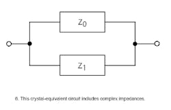
Figure 5b has been redrawn in Fig. 6 to show the complex impedances of the equivalent circuit. The complex impedances2 are defined as:
Combining Z0 and Z1 in parallel yields:
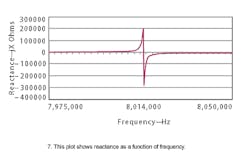
Plugging in the values of Table 2 into a spreadsheet program, the Zp over frequency value is solved and a reactance verses frequency plot can be created (Fig. 7).
This plot shows where the crystal is inductive or capacitive in the circuit. Recall that positive reactances are inductive and negative reactances are capacitive. Between the frequencies fs and fa, the impedance of the crystal is inductive, and at frequencies less than fs and frequencies greater than fa the crystal is capacitive.
As mentioned earlier, the equivalent circuit shown in Fig. 5b is a simplified model that represents one oscillation mode. For this example it is the fundamental mode. The plot in Fig. 7 does not show overtone modes and spurious responses and, as a result, the crystal can appear inductive to the circuit at these overtone modes and spurious responses. Care must be taken in the selection of oscillator components, internal and external, to ensure the oscillator does not function at these points.
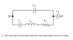
There is no difference in the construction of a series resonant crystal and a parallel resonant crystal, as they are manufactured exactly alike. The only difference between them is that the desired operating frequency of the parallel resonant crystal is set 100 PPM or so above the series resonant frequency. Parallel resonance means that a small capacitance, known as load capacitance (CL), of 12 to 32 pF (depending on the crystal) should be placed across the crystal terminals to obtain the desired operating frequency.3 Figure 8 depicts load capacitance in series with the crystal-equivalent circuit.
Therefore, when ordering a series resonance crystal, CL is not specified and is implied to be at zero. These crystals are expected to operate at in a circuit designed to take advantage of the crystals' mostly resistive nature at series resonance. On the other hand, a parallel resonant crystal has a specified load capacitance. This is the capacitive load the crystal expects to see in the circuit and thus operate at the specified frequency. If the load capacitance is something other than what the crystal was designed for, the operating frequency will be offset from the specified frequency.
Crystal oscillators
A quartz crystal is a tuned circuit with a very-high Q, which, along with many other desirable attributes, makes the crystal an excellent component choice for oscillators. Crystal oscillators are recognizable from their LC oscillator counterparts.1 For the Pierce oscillator, the crystal replaces the inductor in the corresponding LC-tuned circuit oscillators and not surprisingly, the crystal appears inductive in the circuit. Refer to the crystal's equivalent circuit in Fig. 5b when reviewing crystal-oscillator operation.
Upon startup, the amplitude of oscillation builds up to the point where nonlinearities in the amplifier decrease the loop gain to unity. During steady-state operation, the crystal, which has a large reactance-frequency slope (Fig. 7), is located in the feedback network at a point where it has the maximum influence on the frequency of oscillation. A crystal oscillator is unique in that the impedance of the crystal changes so rapidly with frequency that all other circuit components can be considered to be of constant reactance, this reactance being calculated at the nominal frequency of the crystal. The frequency of oscillation will adjust itself so that the crystal presents a reactance to the circuit, which will satisfy the Barkhausen phase requirement.2
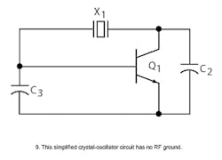
Figure 9 represents a simplified oscillator circuit drawn with only the RF components, with no biasing resistors and no ground connection.
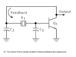
In this design, the inductor has been replaced by a crystal. Looking at the Pierce crystal oscillator, the crystal will appear inductive in the circuit in order to oscillate. The Pierce crystal oscillator (Fig. 10), which is designed to look into the lowest possible impedance across the crystal terminals,3 oscillates just above the series resonant frequency of the crystal.
In the Pierce oscillator, the ground-point location has a profound effect on the performance. Large phase shifts in the resistive-capacitive (RC) networks and the need for large shunt capacitances to ground on each side of the crystal make the oscillation frequency relatively insensitive to small changes in series resistances or shunt capacitances. Additionally, the RC roll-off networks and shunt capacitances to ground provide the circuit with a high immunity to noise minimizing any transient noise spikes.3
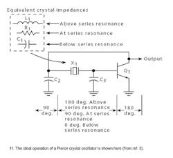
At series resonance, the crystal appears resistive in the circuit (Fig. 11) and the phase shift around the circuit is 2-π radians (360 deg.).
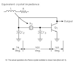
If the frequency of the circuit shifts above or below the series resonant frequency of the crystal, it increases or decreases the phase shift so that the total is no longer equal to 360 deg., thereby maintaining the steady-state operation at the crystal frequency. However, this only happens in an ideal circuit. Under actual circuit operation (Fig. 12), the phase shift through the transistor is typically more than 180 deg. due to increased delay and the tuned circuit typically falls short of 180 deg. Therefore, the crystal must appear inductive to provide the phase shift needed in the circuit to sustain oscillation.
Thus, the output frequency of the Pierce crystal oscillator is not at the crystal-series resonant frequency. Typically, a parallel resonant crystal is specified by frequency and load capacitance, CL. Capacitance CL is the circuit capacitance required by the crystal for operation at the desired frequency. The circuit-load capacitance is determined by external capacitors C2 and C3, transistor internal capacitance, and stray capacitance, CS. A product-design engineer can select the values of capacitors C2 and C3 to match the crystal CL using:
The printed-circuit-board (PCB) stray capacitance can be assumed to be in the range of 2 to 5 pF; it can be minimized by keeping circuit traces as short as possible. A desirable characteristic of the Pierce oscillator is the effects of stray reactances and biasing resistors appear across the capacitors C2 and C3 in the circuit rather than the crystal. If the circuit-load capacitance does not equal the crystal CL, the operating frequency of the Pierce oscillator will not be at the specified crystal frequency. For example, if the crystal CL is kept constant and the values of C2 and C3 are increased, the operating frequency approaches the crystal-series resonant frequency (i.e., the operating frequency of the oscillator decreases). Care should be used in selecting values of C2 and C3. Large values increase frequency stability but decrease the loop gain and may cause problems during oscillator startup. A trimmer capacitor can be substituted for capacitor C2 or C3 to manually tune the Pierce oscillator to the desired frequency. Capacitors with low temperature coefficients, such as NPO or COG types, should be selected for this purpose.
There is much to learn about crystals and crystal oscillators, and this article only covers the basics in an effort to assist the product design engineer in selecting a crystal. More coverage of this topic is available from the Microchip website at www.microchip.com.4 Readers are encouraged to study the design and operation of crystal oscillators because they are such important components in modern electronic designs. Product-design engineers should also consult with a crystal manufacturer about specific product design needs.
REFERENCES
- T.H. Lee, The Design of CMOS Radio-Frequency Integrated Circuits, Cambridge University Press, New York, NY, 1998.
- M.E. Frerking, Crystal Oscillator Design and Temperature Compensation, Van Nostrand Reinhold Co., New York, 1978.
- R.J. Matthys, Crystal Oscillator Circuits, Revised Ed., Krieger Publishing Co., Malabar, FL, 1992
- Application Note AN826, "Crystal Oscillator Basics and Crystal Selection for rfPIC™ and PICmicro® Devices," Microchip Technology, Chandler, AZ, Internet: www.microchip.com.
This file type includes high resolution graphics and schematics when applicable.
