Designing Wideband RF Impedance Transformers
This file type includes high resolution graphics and schematics when applicable.
Impedance matching devices are often used in high-frequency circuits, typically to match the impedance of a device or component to the characteristic impedance of a circuit or system. In some circuits, it is desirable for the impedance matching to achieve multiple-octave frequency coverage accompanied by low insertion loss. To help designers working with impedance transformations, this article explores the design of unbalanced-to-unbalanced (unun) wideband impedance transformers with an impedance ratio of 1:4. Such transformers are useful in radio communications systems, typically in hybrid circuits, signal combiners and dividers, and for interstage coupling of amplifier chains.
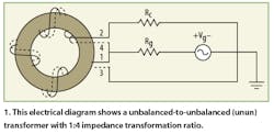
Such wideband unun impedance transformers are also useful for test circuits, optical receiver systems,1 microwave circuits with wideband impedance matching,2 and antenna coupling.3 Modern computational programs usable for high-frequency circuit design and simulation include this device in their tool boxes.4 A wideband unun impedance transformer consists of a toroidal ferrite core wrapped with a twisted bifilar transmission line, with the wires isolated by means of an enamel film. By combining design elements of conventional and transmission-line impedance transformers, it is possible to create a true wideband component. The design offers high efficiency for an impedance transformation ratio of 1:4 (Fig. 1).5
Conventional
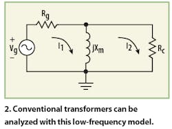
In a conventional impedance transformer, the energy transference between the primary and secondary windings occurs mainly through magnetic coupling which also accounts for the transformer's capability of providing good low-frequency response. Assuming a lossless ferrite core and purely resistive load and source impedances, and considering only the influence of its magnetization inductance, the simplified low-frequency model for the transformer can be represented by the structure in Fig. 2.6,7
The low-frequency model response under maximum power transference condition is determined by the device's insertion loss:
where:
Pg = the maximum available power of the source,
Pc = the power delivered to the load,
Rg = the source impedance, and
Xm = the magnetization reactance. This last parameter is determined by the operating frequency, f, and the core magnetization inductance, Lm, through:
The value of Lm depends on the number of turns for the primary winding and a core inductance factor, Al. Usually, this factor is specified by ferrite core manufacturers in nanoHenries/turns squared (nH/turns2). Therefore, the magnetization inductance in nH is:
By applying this parameter within the corresponding reactance formula, and substituting the result of that calculation into the insertion loss equation, the lower cutoff frequency of the transformer can be determined by putting the relationship in Eq. 2. Therefore:
This value decreases as the number of turns for the primary winding increases. This formula can also be applied for a given desired cutoff frequency in order to calculate the proper number of turns for the primary winding. The factor of 109 is used so that the inductance specification ca be presented in nH.
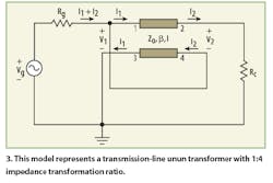
The electrical coupling between the primary and secondary windings of a transmission-line transformer improves the transfer of high-frequency energy. Figure 3 shows the high-frequency model for a transmission-line 1:4 unun transformer, considered without losses because of its short length.5
In this idealized model, the source and load impedances are assumed to be pure resistances. The high-frequency model response is quantified also by its insertion loss. Again, the ratio between the available source power and the secondary load power is:
where:
Rg = the source impedance,
Rc = the load impedance,
Zo = the transmission-line characteristic impedance,
β / = the phase factor, and
l = kλ = the length of the transmission line with k a fraction of wavelengthλ.
Equation 5 shows the importance of an optimum Zo value to achieve good wideband high-frequency response. The power transference is nullified for a half-wavelength (λ/2) line length, and will be 1 dB less than the maximum value for a quarter-wavelength (λ/4) line length. From this is can be seen that shorter lengths of line result in broader-bandwidth high-frequency responses. The optimum line characteristic impedance and the load impedance for maximum power transmission are:
A 1:4 transformation is necessary between the source and load impedances for impedance matching. With this result, a relationship between line characteristic impedance and the source and load impedances can be established:
Twisted transmission line
The use of twisted transmission line in a transformer makes it possible to set the characteristic impedance almost at an optimum value for a desired passband by varying the number of twists per unit length of transmission line. An increase in the number of twists per unit length results in a decrease in the characteristic impedance.
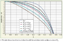
Figure 4 plots insertion loss behavior as a function of k for optimized and non-optimized values of characteristic impedance. For a case with non-optimized characteristic impedance, the insertion loss increases and bandwidth decreases relative to a case using optimized characteristic impedance.
Thus, the use of twisted transmission line is readily justified for obtaining optimum values of characteristic impedance.8,9
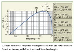
As a comparison, simulated performance was predicted using the Advanced Design System (ADS®) computer-aided-engineering (CAE) software suite from Agilent Technologies (www.agilent.com) while design prototypes were measured with a commercial microwave vector network analyzer (VNA). The analysis indicated the relationship between the load and source power.
In order to determine a transformer's low-frequency response, the characteristics of the ferrite core must be known since the inductance factor Al is determined relative to a specific frequency. Knowing this as well as the source's internal impedance (Rg), a designer can establish the low-frequency cutoff frequency (fi) and, using Eq. 4, can calculate the required number of turns (Np) for the primary winding. To determine the high-frequency response, information about the transmission line is required, such as its characteristic impedance (Zo), the propagation velocity (vp), and the phase factor (β), all at the desired operating frequency. Along with the values of the source impedance (Rg) and the load impedance (Rc), the optimum theoretical value of the characteristic impedance (Zopt) can be determined by applying Eq. 6. Knowing the characteristics of the transmission line, the high-frequency cutoff frequency (fs), and the true characteristic impedance of the transmission line, Zo, it is possible to calculate the propagation velocity (vp) and the phase factor (β). With the value of the true characteristic impedance, Zo, the difference between it and Zopt can be verified and the definitive insertion loss for fs be specified. Figure 4 shows the determination of values of k as a function of true characteristic impedance (Zo) and insertion loss. With values for k, vp, and fs , the line length (l) required for achieving the previous specifications can be calculated through:
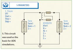
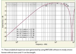
MATLAB mathematical analysis software from The MathWorks (www.mathworks.com) was used to analyze the response of the transformer device model.10 In this analysis, the insertion-loss responses for the individual low-frequency (Eq. 1) responses and high-frequency (Eq. 5) responses were combined. The desired target values were substituted into the MATLAB equations to obtain the final response of the wideband transformer. To achieve an electrical simulation of the MATLAB model's numerical response, the ADS modeling software was used. The software features a useful internal model for the source, called XFERRUTH, with variable parameters that include the number of turns (N), the inductance factor (AL), the characteristic impedance of the line (Z), the electrical length of the transmission line (E), and the reference frequency (F) for the calculation of the transmission-line length.
In order for ADS to performance a device simulation on the transformer with the responses as scattering parameters (S-parameters), it employs its S_Param modeler, adjusting the initial (start) and the final (stop) sweep frequencies according to a specified step size. and the graduation step size. The source and load impedances are represented by a specific termination called Term, with an impedance value of Z. Figure 5 shows the circuit that was used in the ADS simulation.
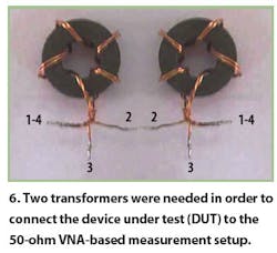
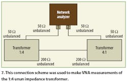
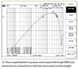
Measurements were performed on a commercial VNA from Advantest (www.advantest.com), a 300-kHz-to-3.8GHz model R3765CG. The analyzer features unbalanced test ports with terminal impedance of 50 ohms. Since the wideband unun impedance transformer has unbalanced terminals and a transformation ratio of 1:4, another device with 4:1 transformation ratio was needed to perform the impedance conversion needed to adapt the device to the measurement equipment. Figures 6 and 7 show all the terminals connections.
Both test terminals and all cables used with the VNA were calibrated in order to minimize their error contributions. The insertion loss and the passband response were analyzed by means of transmission coefficient S21 measurements presented in log-magnitude form.
Measurement conditions
The comparative results among the analytical (MATLAB), numerical (ADS), and the experimental models were obtained under several measurement conditions. A model E1003C5 toroidal ferrite core from Sontag Componentes Eletronicos (www.sontag.com.br) was used in the experiments. Its geometric and electromagnetic data include an external diameter of 10 mm, an internal diameter of 5 mm, a width of 3 mm, relative permeability (µr) of 11, and an inductance factor (Al) of 4.2 nH/turns2 .11 It is specified for use in the frequency range from 500 kHz and 50 MHz. A five twists per centimeter line with 30AWG-conductor transmission line was used. At 130 MHz, this line has a 38-ohm characteristic impedance, phase factor (β) of 4.5501 rad/m, and propagation velocity (vp) of 1.7952 X 10⁸ m/s. The optimum value of the characteristic impedance for a 50-ohm source impedance must be 100 ohms, given in Eq. 8, meaning a 0.38 times relationship. The k value for this difference and a insertion loss of 3 dB is 0.2207.
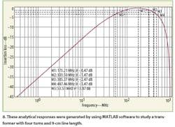
The first device was fabricated with four turns, resulting in a 9-cm line length. Figures 8, 9, and 10 show the frequency insertion loss behaviors for analytical, numerical, and experimental cases.
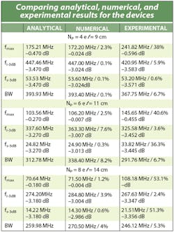
The table summarizes the main values, including insertion-loss results at maximum amplitude, at –3 dB frequencies (fmax, fi-3dB, and fs-3dB), the proper bandwidth (BW), and the percent frequency differences compared to model values. The differences among the analytical, numerical, and experimental results are very small, except at the maximum signal frequency. This can be attributed to limitations in the test system caused by noise and other parasitic effects in the measurement setup. Across the test frequency band with essentially constant amplitude, variations in signal level are imperceptible, perhaps accounting for differences in reporting the maximum signal amplitude frequency.
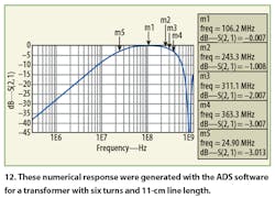
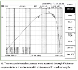
A second device was constructed with six turns and 11-cm line length. With the increase in the number of turns, the lower cutoff frequency decreases and the higher cutoff frequency is also lowered as a result of the increased line length. For the lower cutoff frequency, the values of the analytical and numerical results were as expected. However, the experimental responses do not agree exactly with the theoretical model. The values of the high-frequency responses are as expected, with good agreement among the three sets of values. Figures 11, 12, and 13 show insertion loss as a function of frequency for the analytical, numerical, and experimental cases (shown also in the table).
There is a small difference between the analytical and numerical results, due to the inherent limitations of the model. On the other hand, the experimental results prove the validity of the model, except at the low-frequency limit, where the largest error occurred. This is due to the fact that the theoretical model does not account for all of the parasitic elements of the components used in the constructed transformers.
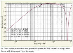
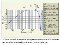
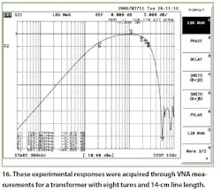
For a further comparison, a transformer with eight turns and 14-cm line length was constructed. The results of the analytical, numerical, and experimental cases are summarized in the table and shown in Figs. 14, 15, and 16.
At the lower cutoff frequency, the analytical and numerical cases agree but the experimental results do not agree with the theoretical model. However, the higher cutoff frequency values are close to either other and to the expected results. As the number of turns was increased, the lower cutoff frequency was reduced; similarly, as the line length increased, the upper cutoff frequency was also reduced.
Summary
Although the three sets of results were determined by different methods, they appear satisfactory and in good agreement with each other. The analytical (MATLAB) and numerical (ADS) model responses and the experimental responses (VNA measurements) compared closely. The analytical and numerical cases yielded approximately the same values, with some differences compared to the experimental results. This is best explained by the fact that the theoretical models do not fully account for the complex characteristics of the components used in the fabrication of the transformers, which were modeled as more or less "ideal" components.
These model equations represent a simplified equivalent-circuit model for a coil transformer. Recent studies have shown the need to use a more elaborate model that includes resistive and reactive effects as a function of increasing frequency and number of turns.12
These advanced models also include the effects of inter-winding capacitance, which decreases the self-resonant frequency of the inductor. Still, these simplified design equations can provide reasonable results, replacing the more involved empirical processes usually involved in the design of a 1:4 impedance transformer. As these simplified equations show, they can be used to design transformers over a wide frequency range (three octaves) with low insertion loss and at low cost.
REFERENCES
- M. Dong, and H.D.S. Salvy, "Analyzing 4:1 TLTs for Optical Receivers," Microwaves & RF, March 2005, Vol. 45, No. 1.
- I.J. Bahl, "Broadband and Compact Impedance Transformers for Microwave Circuits," IEEE Microwave Magazine, August 2006, Vol. 7, No. 4, pp. 56-62.
- The ARRL Handbook for Radio Communications, 82 ed., The American Radio Relay League Inc., Newington, CT, 2005.
- Advanced Design System (ADS) 2004C, Agilent Technologies (www.agilent.com), 2004.
- C.L. Ruthroff, "Some Broad-Band Transformers," Proceedings of the IRE, August 1959, Vol. 47, No. 8, pp. 13371342.
- J. Sevick, Transmission Line Transformers, 4th ed., Noble Publishing, Atlanta, GA, 2001.
- J. Sevick, "A Simplified Analysis of the Broadband Transmission Line Transformer," High Frequency Electronics, February 2004, pp. 48-53.
- A.A. Ferreira, Jr. and W.N.A. Pereira, "Ensaios experimentais com Transformadores Banda Larga em RF," in Proceedings of the World Congress On Computer Science, Engineering and Technology Education-WCCSETE'2006, Santos, Sao Paulo, Brazil, 2006, pp. 473-477.
- A.A. Ferreira, Jr., "Projeto de transformador de impedancia de radiofrequencia com controle da faixa de passagem," Dissertacao de Mestrado, Instituto Nacional de Telecomunicacoes, Santa Rita do Sapucai, Minas Gerais, Brazil, 2006.
- MatLab 7, The MathWorks, Inc. (www.mathworks.com), 2005.
- SONTAG, Sontag Componentes Eletronicos, Disponivel (www.sontag.com.br).
- L. Green, "RF inductor modeling for the 21st century," EDN, September 2001, pp. 67-74.
This file type includes high resolution graphics and schematics when applicable.

Leaders relevant to this article:


