Download the PDF of this article.
Microstrip transmission lines serve high-frequency circuit designs on a wide range of substrate materials, but CMOS-grade silicon may not be the first to come to mind. Still, silicon is a low-cost foundation for analog and digital integrated circuits (ICs), and it may provide a useful starting point for miniature microstrip-based passive components, such as filters and antennas. But first, it is necessary to understand the loss characteristics of microstrip on silicon dielectric material, whether working on lower-frequency RF, microwave, or digital circuits. Proper analysis of the loss mechanisms can yield more accurate predictions of final circuit performance levels.
In microstrip circuits, the electromagnetic (EM) fields propagate mostly through the conductive metal circuit traces and the dielectric material, such as silicon. But a small portion of the EM energy also travels through the air above the microstrip circuit’s conductors, resulting in an inhomogeneous medium and quasi-transverse-EM (quasi-TEM) mode propagation. The inhomogeneous nature of a microstrip circuit structure makes quasi-static approximations of analyzed TEM-coupled transmission lines difficult and limits its accuracy.1
Most of the signal attenuation in a microstrip transmission line is due to the finite conductivity of the conductor metal and the dielectric loss of the substrate material.2,3 The amount of signal attenuation depends on a number of factors, including the properties of the substrate material, the properties of the conductor metal, and the operating frequency range. Microstrip transmission lines can also exhibit radiation losses, as well as losses at any air-dielectric interfaces without conductors. Radiation loss can be minimized by the use of thin and high-dielectric-constant circuit materials.
Conductor losses are typically greater than the other losses exhibited by microstrip circuits. However, as the operating frequency increases, dielectric losses become a larger part of the loss budget. In the case of a substrate material with high loss, such as CMOS grade silicon, the effects of dielectric and surface-wave propagation are more dominant than conductor losses. Simulation software based on the finite-element method (FEM) can model many of the parasitic effects that affect microstrip losses, but FEM software may not account for all attenuation mechanisms in microstrip circuits, resulting in the possibility of differences between measured and simulated results.
Analysis of microstrip loss mechanisms can provide guidance on using microstrip with silicon substrate materials. Equation 1 presents phasor notation for the frequency-domain signal propagation in a transmission line:
Ē(f,z) = E(f,z)e –[α(f)+β(f)]z (1)
where Ē(f,z) is the Fourier transform of the time-domain waveform at a distance z; α(f) is the frequency-dependent attenuation; and β(f) is the frequency-dependent phase responsible for signal dispersion. By focusing on the attenuation mechanism represented by α(f), involving conductor, dielectric, and radiation losses, the impact of substrate permittivity on loss can be understood. Substrate selection is critical for a circuit design, since dielectric constant will dictate the required circuit dimensions for a target line impedance along with frequency. But it is not simply a matter of choosing a material with higher dielectric constant to design smaller circuit dimensions: Substrates with higher dielectric constants typically exhibit greater losses than materials with lower dielectric constants.
1. The diagram depicts a microstrip transmission line with conductor width w and height h, enclosed in a box not considered as part of the loss analysis.
Figure 1 shows a microstrip transmission line with conductor width w and height h, enclosed in a box not considered as part of the loss analysis. Dielectric constant is the key material parameter involved in quantifying the intrinsic capacitance between conductors. In time-varying electric fields, dielectric loss represented by the substrate material’s loss tangent is taken into consideration. Due to the field distribution in microstrip, the effective dielectric constant, ɛeff, has a lower value than the relative permittivity or relative dielectric constant, εr, of the substrate material. The effective dielectric constant, εeff, can be found by means of
εeff = C/Ca = (c/vp)2
where C is the capacitance of the microstrip on a dielectric material and Ca is the capacitance of the microstrip structure considering vacuum in place of the dielectric.
A general expression for ɛeff is
ɛeff = [(ɛr + 1)/2] + [(ɛr – 1)/2]{(1 + 10(h/W)−0.5 + 0.041[1 – (W/h)]2}
for W/h >> 1. The equation for effective dielectric constant has been generalized in considering only a perfect dielectric constant (with σ = 0 and ω = 0). The influence of frequency on effective permittivity is shown in Eq. 2:
εeff (f) = εr − (εr − εeff)/[1 + G(f/ft)2] (2)
where
G = [(Z0 – 5)/60]0.5 + 0.004Z0 and ft = 15.66(Z0/h)
with ft in GHz, h in mils, and Z0 in Ω.
At higher frequencies, the value of ɛeff approaches the value of ɛr for a microstrip substrate, implying that most of the energy propagates through the substrate (and less through the air) at higher frequencies. Considering finite metal thickness, Eq. 2 can be rewritten as Eq. 3:
ε′eff = εeff – [(εr – 1)/4.6][(t/h)/(W/h)0.5] (3)
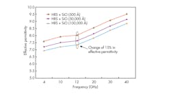
where t/h ≤ 0.2; 0.1 ≤ W/h ≤ 20; and εr ≤ 16. Figure 2 shows the influence of the substrate passivation layer thickness on the effective permittivity, and how variations increase with frequency. High-resistivity silicon substrates with various oxide thicknesses were used in this analysis.
2. The passivation layer thickness has a determination of the effective permittivity of silicon substrate.
It is important to note that εr for a given material is a complex quantity. Equations 4 and 5 represent the complex value of the dielectric constant:
∇ × H = J = JD + JC = jωD + JC = jω[εʹ – jεʺ – j(σ/ω)]E = jωε*E (4)
ε* = [εʹ – jεʺ – j(σ/ω)] (complex dielectric constant) (5)
for σ = 0, where
Parameter εʹ is known as ac capacitance of the dielectric material; εʺ is the dielectric loss factor and represents dielectric absorption; and δ is the dielectric loss angle associated with molecular motion and relaxation. This relation assumes matter to be linear, having time lag for atomic particles to respond to frequency variations. Furthermore, it shows that the electric and magnetic fields in the dielectric material are no longer in time phase.
The dielectric loss tangent, tan δ, can be shown to equal
tan δ = εʺ/ εʹ
or
tan δ = (εʺ/ εʹ) + (σ/ωεʹ) for dielectric material with high loss.
Frequency variations in the values of εʹ and εʺ depend upon the characteristics of the dielectric material. In the case of a vacuum, εʺ = 0. In the case of a merely good dielectric material, such as polytetrafluoroethylene (PTFE), εʹ is constant and εʺ exhibits a small, incremental increase with frequency. A lossy dielectric material, such as silicon, has a value of εʹ decaying at higher frequencies and considerably larger value of εʺ decaying at RF. In the case of a silicon dielectric material, a loss tangent of 0.005 at 1 GHz increases to 0.015 at 10 GHz, indicating different phenomena than for insulator material, where the overall permittivity decreases with increasing frequency. Considering ɛ0 as the dielectric constant of a vacuum and A as the capacitive area of a conductor with metal thickness t, the relative dielectric constant, εr , can be written as:
εr = ε*/ε0 = [εʹ − jεʺ - j(σ/ω)]/ε0 = εʹr − jεʺ = Ct/ε0A (6)
Parameter εr is frequency dependent, although the variations with frequency tend to be gradual and often fairly constant over a narrow band of frequencies. Variations of the loss tangent, tan δ, with frequency are more pronounced. The imaginary part of Eq. 6 accounts for the damping of the vibrating dipole moments. As shown in Eq. 4, the induced current density for the linear case (J) can be given as:
J = [σ + jω(εʹ − jεʺ)]E = [(σ + ωεʺ) + jωεʹ]E (7)
The real part of the first term is known as the dissipative current; it is associated with the power loss of a microstrip substrate. The imaginary part of this current is known as reactive current associated with the stored energy. In the case of a semiconductor, it is assumed that the dissipative current is equal to the reactive current density. Dielectric loss is represented by the loss tangent, tan δ, as shown in Eq. 8:
tan δ = (ωεʺ + σ)/ωεʹ = tan δd + tan δL (8)
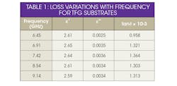
In general, loss tangent term tan δL is considered negligible; the only significant loss contributions come from loss tangent term tan δd. Loss tangent term tan δd results from the polarization loss associated with the intrinsic substrate characteristics, while tan δL is defined as the extrinsic loss resulting from the finite conductivity of the substrate material, which is applicable for silicon substrates. The value of the dielectric constant is affected by various other factors, such as temperature and humidity. Table 1 lists variations in loss with frequency for TFG substrate.4
A number of approaches are available for measuring the dielectric constant of a material, including the coaxial line method, the resonant cavity method, the Von-Hipple method, the Heston and Smythe method for liquids, the Surber method for liquids, and Poly’s method for high-loss liquids. For stacked substrates, the total permittivity of the structure (εT) can be calculated by means of Eq. 9:
εT = tT[(t1/ε1) + (t2/ε2) + (t3/ε3) + …] −1 (9)
where tT is the total stacked thickness; t1, t2, and t3 are the thicknesses of the individual substrate layers; and ɛ1, ɛ2, and ɛ3 are the permittivities of those substrate layers, respectively. The wave impedance, Ẑ, can be found by using Eq. 6 to show the following:
Ẑ = [Z0/(εʹ)0.5][(cos δ/2 + jsin δ/2)/(1 + tan2 δ)0.25]
Propagation delays affect the performance of high-speed computer logic and high-bit-rate digital communications circuits and systems, and circuit material permittivity plays a role in circuit propagation delays. Considering homogenous and nonmagnetic dielectric media, the propagation delay time per unit length, td, is
τd (ns/mm) ~ 3.62(εr)0.5 (10)
In CMOS, the gate length is chosen according to the appropriate associated propagation delay. Silicon substrates are not often used for high-frequency applications due to the significant attenuation at high frequencies. The main losses stem from the substrate and surface mode propagation. The low-resistivity silicon substrates used for CMOS processing are not used for RF circuits, since the parasitic EM signal propagation through the substrate causes considerable noise and crosstalk at RF. Crosstalk increases with frequency as a result of substrate coupling effects. Substrate resistance dominates signal propagation performance at moderate frequencies, while the capacitance/permittivity of silicon substrates plays more of a role at higher frequencies.
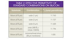
To use silicon substrates at RF and achieve better isolation, crosstalk, and noise suppression, thick oxide layers or isolation structures are usually employed. Silicon-on-insulator (SOI) materials can usually provide good isolation, although with more self-heating effects than standard silicon. Partial SOI materials can be employed, but they require chemical/mechanical polishing. High-resistivity silicon with low doping (using float zone processing) achieves limited isolation at multiple-GHz rates, compromising integration density due to limited junction isolation. In contrast, bulk micromachining allows removal of silicon locally, such as beneath an active device, although this approach leads to fragile device structures and higher radiation losses due to lower effective permittivity with the removal of silicon material (Table 2).
Working with Silicon
CMOS-grade silicon is not considered a good conductor or a good dielectric due to its limited conductivity and resistivity. Through experimentation, however, it was found that silicon material with a thickness of 5 μm above standard grade was sufficiently thick to overcome substrate losses at lower frequencies. The interface above the silicon substrate (typically oxide and nitride layers) is considered as metal-insulator-semiconductor (MIS), as shown in Fig. 3. It supports three modes of propagation: skin-effect mode, dielectric quasi-TEM mode, and slow wave mode. Standard resistivity silicon (ρ ~ 10 to 20 ῼ-cm) supports skin-effect-mode propagation due to its low conductivity.5 Higher resistivity silicon ( >1 kῼ-cm) supports quasi-TEM mode propagation, whereas moderate operating frequency and resistivity leads to slow-wave-mode propagation.5
3. Micromachining allows the removal of small amounts of silicon beneath active devices for microstrip circuits fabricated on silicon substrates.
Standard resistivity silicon is not suitable for RF applications since the higher operating frequencies result in excessive signal attenuation due to dielectric losses.6 Conductor losses are not affected by the substrate resistivity and major loss contributions at RF are from dielectric losses, as well as surface-wave propagation. Free charge carriers cause the main part of the losses in the semiconductor material and, as seen from Eq. 8, the main loss contribution is from the finite conductivity. Employing high resistivity silicon reduces the attenuation, with increase in resistivity by an order of one decreasing attenuation by one-half at C-band frequencies. The functional cutoff frequency for passive circuits is given by:
fc = 1/(2πρεʺ)
with ρ = 1/(qnµ), where q is the charge concentration, n is the number of half-wavelengths, and µ represents the charge mobility.
The transition frequency of a material, fc, depends on the resistivity (ρ = 1/σ) which is determined by the doping level of the material. Conductivity is an important semiconductor parameter, depending upon the doping concentration and carrier mobility in contrast to a conductor. Bias also plays an important role in the MIS structure with the introduction of interface losses at the interface between the dielectric (oxide) and the silicon substrate. In addition to substrate losses, losses occur in the depletion, accumulation, and inversion regions.
4. This is a depiction of a silicon substrate with an interface layer.
For a silicon substrate, the losses are primarily from the substrate and interface losses occurring between the insulation layer and silicon substrate (Fig. 4). These losses can be minimized by employing a high-quality gate oxide with a high-resistivity silicon substrate. For 10-kΩ-cm resistivity silicon, substrate losses are 0.032 dB/cm, increasing to 32 dB/cm for material with resistivity of 10 ῼ-cm.7 Micromachining is generally performed on silicon substrates to minimize losses associated with the substrate. The removal of silicon substrate material by micromachining produces a net decrease in effective permittivity, with a resulting increase in radiation losses (Table 3).
Generally, conductor losses in microstrip are having the major contribution due to skin depth. Skin effect concentrates current near the conductor surface along with edge effects, resulting due to increased resistance. This phenomenon takes place at the frequency at which conductor thickness is higher than the skin depth. The critical frequency at which a conductor makes a transition from electrically thick to electrically thin is
fcrit (Hz) = 4/πμ0t2 (11)
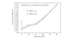
Figure 5 shows the simulated response of the variation of the metallization thickness on the conductor loss on the high resistivity silicon substrate with a 0.5-μm-thick oxide passivation layer. The effect is prominent to 20 GHz but minimized due to skin effect phenomena. This phenomenon also occurs for the transmission lines with width smaller than its thickness, in which the current flows on the sides rather than the top and bottom of the conductor. But in silicon substrate this loss is higher because of the finite metallization thickness due to process constraints.8
5. Metallization thickness affects the amount of conductor loss for a silicon substrate.
Compared to standard alumina substrate having attenuation of 5 × 10⁻⁴ (10 GHz), the silicon losses changes with the resistivity considerably. High resistivity silicon substrate (1 k ῼ-cm) is having attenuation of the order of 10−3 compared to 10−4 for silicon with resistivity of 10 kΩ-cm. Higher-speed devices having pulses with rise time faster than 1 ns, metallization thickness of 10 um makes skin depth comparable with the thickness and cause signal degradation. Conductor attenuation (αc) can be described as:
αc = 0.072[(f)0.5/wZ0]λg (dB)/λg
= (8.686/wZ0)(πfμ/σ)0.5 (dB)/m (12)
where f is in GHz.
In terms of quality factor, conductor attenuation is:
αc = 8.68βn/Qu (dB/mm) (13)
where Qu = QL/(1 – 10−(IL/20))
where βn = 2π/lg and n is the number of half-wavelengths.
The quality factor associated with the attenuation constant, Qc, can be written as:
Qc = 27.3/αc ≈ 0.63h(σf)0.5 (in GHz)
The dielectric attenuation constant attached with the loss can be expressed9, 10 as:
αs = 27.3[εr(εeff – 1)tan δ]/[εeff(εr – 1)][(tan δ)/λg] in dB/λg (14)
where
λg = λ0/(εeff)0.5
The total attenuation can be written as α = αc + αs. For silicon, the total attenuation is α = −αc + αL +
αd. The quality factor associated with the attenuation constant, Qs, can be written1 as:
Qs = 27.3/αs ≈ 1/(tan δd + tan δL);
1/Q = 1/Qc + 1/QS;
Q = (β/2α)([λ0(αc + αs)]/{π[εeff (f)]0.5})
tan δ = tan δd + tan δL = εeff(εr – 1)/[Qsεr(εeff – 1)]
The power radiated from any discontinuity can be modelled as shunt conductance, Grad :
Grad = (60π2/Z02)(h/λ0)2 ((8/3εeff)[1 + (4/5εeff) – (1/εr)] + …)
The radiation becomes significant at higher frequencies according to the relationship:
fh >2.14(εr)0.25
where f is in GHz and h is in millimeters.
High-resistivity silicon with a 5-μm oxide layer deposited by plasma-enhanced chemical vapor deposition (PECVD) has higher attenuation for microstrip than standard alumina substrates (about 0.06 dB/mm), although somewhat less than the 1 dB/mm attenuation in microstrip lines on standard silicon substrates characterized at X-band frequencies.
Propagation of surface waves in the dielectric material contribute to the overall attenuation in microstrip lines. A dielectric sheet on a ground plane acts as a guiding structure for surface waves.11 The electric field at the bottom surface is considerably high, which leads to the excitation of the substrate mode. The waves may propagate in any direction parallel to the surface. Transverse-magnetic (TM) mode, which is the lowest-order mode with no cutoff frequency, will propagate to DC, but is weakly guided by the surface. Since the propagation coefficients for this surface-wave mode and the normal microstrip quasi-TEM mode are different, coupling between the modes is negligible. At lower frequencies, the majority of energy is transmitted above the substrate so that ɛeff ~ 1. At higher frequencies, ɛeff for the surface wave increases, resulting in coupling between the modes resulting in comparable phase coefficients. The lowest frequency, fL, at which coupling to a surface-wave mode may occur, is:
fL = c arctan(εr)/πh[2(εr – 1)]0.5 (15)
To avoid surface-wave propagation, microstrip circuits are operated below fL. The phenomena is predominant for narrow microstrip lines; for wider microstrip lines, transverse microstrip resonance may occur, which can also be suppressed by the use of narrow longitudinal slots in the metal strip.
Silicon is a low-cost substrate material with potential for RF/microwave microstrip circuits, provided that the loss mechanisms of the circuit structures are fully understood. Substrate permittivity is a complex parameter that has a huge impact on microstrip on silicon loss mechanisms, but it is a parameter that has been thoroughly analyzed, with much information available.
Accurate dielectric properties, including dielectric constant and intrinsic dielectric loss tangent, are essential for designing microwave integrated circuits on silicon. Along with the above, present-day circuits having RFIC and RFCMOS concept on silicon need accurate prediction of the losses associated with the substrate to reduce the turnaround time in multiple iterations.
Kamaljeet Singh, Scientist/Engineer, Systems Engineering Group
A.V. Nirmal, Group Director, Systems Engineering Group
S.V. Sharma, Deputy Director
ISRO Satellite Centre, Bangalore, India
Acknowledgment
The authors gratefully acknowledge the director of ISAC for his support and encouragement.
References
1. S.Y. Liao, Microwave Devices and Circuits, Prentice Hall, Englewood Cliffs, NJ.
2. David M. Pozar, Microwave Engineering, 2nd ed., John Wiley & Sons, New York, 1998.
3. T.C. Edwards, Foundations for Microstrip Circuit Design, John Wiley & Sons, New York, 1991.
4. L. Mruthyunja and K.N. Suryanarayana Rao, “Measurement of dielectric constant of aerospace dielectric materials,” Journal of Spacecraft Technology, Vol. 6, No. 2, 1996, pp. 28-31.
5. Kamal Benaissa, J.-Y. Yang, D. Crenshaw, S. Sridhar, et al. “RF CMOS on high resistivity substrates for system-on-chip applications,” IEEE Transactions on Electronic Devices, Vol, 50, No. 3, March 2003, pp. 567-576.
6. R.-Y. Yang, C.-Y. Hung, Y.-K. Su, M.-H. Weng, and H.-W. Wu, “Loss characteristics of silicon substrate with different resistivities,” Microwave and Optical Technology Letters, Vol. 48, No. 9, September 2006, pp. 1,773-1,776.
7. C. Schollhorn, W. Zhao, M. Morschbach, and E. Kasper, “Attenuation Mechanisms of Aluminum Millimeter-Wave Coplanar Waveguide on Silicon,” IEEE Transactions on Electron Devices, Vol. 50, No. 3, March 2003, pp. 740-746.
8. James C. Rautio, “An investigation of microstrip conductor loss,” IEEE Microwave Magazine, December 2000, pp. 60-67.
9. Ramesh Garg and K. C. Gupta, Computer-Aided Design of Microstrip Circuits, Artech House, Norwood, MA, 1981.
10. Panagiotis Sarafis, Emmanouel Hourdakis, and Androula G. Nassiopoulou, “Dielectric Permittivity of Porous Si for Use as Substrate Material in Si-Integrated RF,” IEEE Transactions on Electronic Devices, Vol, 60, No. 4, April 2013, pp. 1,436-1,443.
11. E.H. Fooks and R.A. Zakarevicius, Microwave Engineering Using Microstrip Circuits, Prentice-Hall, Englewood Cliffs, NJ.


