Design of a Dual-Band PA for Millimeter-Wave 5G Applications
Download this article as a .PDF
Considerable time and money are currently being invested in developing millimeter-wave technology for 5G, and there is much debate and lobbying in regard to the most suitable frequency bands for this application. In the U.S., the FCC has allocated licensed spectrum at 28 GHz, 37 GHz, and 39 GHz. In Europe, the Radio Spectrum Policy Group (RSPG) has recommended the 26-GHz band (24.25 to 27.5 GHz) as the pioneer band for 5G, with all the EU member states making a portion of this band available for 5G. It also recognized that the 32-GHz band (31.8 to 33.4 GHz) could be made available by many European administrations and effort should be made to keep it as an option for 5G in the future.
Development work is currently underway in all of these bands, and it is looking increasingly unlikely that a single band will be designated on a worldwide basis for millimeter-wave 5G in the immediate future. This means that the availability of dual-band or multi-band millimeter-wave components will become increasingly attractive.
This article describes the design, layout, and performance of a dual-band power amplifier (PA) monolithic microwave integrated circuit (MMIC), capable of electronically switching its operating band between the 26-GHz and 32-GHz bands. The starting point was to undertake the preliminary design of two standalone PAs, each addressing one of the target bands. The targeted output power was 1 W at 1-dB gain compression (P1dB)—a commercially available 0.15-µm gate length pHEMT process was selected to achieve this. A three-stage design was implemented to achieve a small signal gain of around 20 dB.
PA Design Process
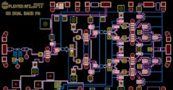
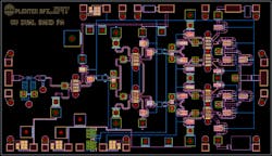
The design of each PA commenced with the selection of the output transistor size and bias. Increasing the total gate width of the selected transistor also increases the available RF output power. However, the higher parasitics of the physically larger transistor result in a reduction in available gain. The proven design approach to address this is to use multiple power-combined transistors. To achieve the target output power, a total of four eight-finger transistors were power-combined in the output stage. This output stage was driven by a pair of devices, and this in turn was driven by an input stage realized using a single transistor. The topology adopted is evident from the layout plot of the dual-band PA (Fig. 1).
It was necessary to adopt certain commonalities in the initial design of the two PAs. The transistor sizes in each stage needed to be identical, and the basic power-combining topology needed to be similar. It was also necessary to have some degree of commonality in the matching structures used in the two PAs. However, some differences in the structures could be accommodated as part of the dual-band implementation—this versatility allows freedom to optimize the performance in both bands.
Band Switching Approach
Converting the two individual PA designs into a single switched design commenced at a relatively early stage in the design process. The basic approach was to switch certain RF elements in and out of the circuit. pHEMT transistors can be used to realize good RF switches by biasing the drain-source voltage (Vds) at 0V and controlling the gate bias voltage.1
Figure 2 depicts a simple equivalent circuit for a pHEMT operating as a switch. The resistance varies from a low value with the gate at 0 V to a high value when the transistor is pinched off. This provides a simple but effective switching function, which is the basic means of realizing RF switches.
The problem with using pHEMTs as millimeter-wave switches is the parasitic capacitance. This capacitance can be lowered by reducing the total gate width of the switching transistor, but that in turn increases the insertion loss. The basic structure of the pHEMT—with its parallel drain and source fingers—means that pushing the parasitic capacitance to very low levels results in small transistors that have very high insertion loss and poor linearity. Even a capacitance of just 0.1 pF has an isolation of just 1 dB at 31 GHz.
The key to implementing the RF switches in the dual-band PA was to consider them not as ideal switching elements but as varying reactance elements. The reactance was absorbed into the PA matching structures such that the switch parasitics became an integral and required part of the matching networks. The matching networks of the two PAs were reviewed individually from output to input.
It was necessary to adopt common positions for certain key matching elements such as the drain bias feeds, which were configured with switching elements to shorten the effective electrical length in the higher band implementation. It was possible to retain some matching elements as common for both bands, but others were switched in or out as appropriate. The key in all cases was to adopt a topology that could accommodate the switch parasitics in both bands.
The process of implementing switchable matching structures throughout the entire amplifier required great care and attention to detail. Much effort was expended on keeping the number of switching elements down to an acceptable level. If the number of required switching elements becomes excessive, the size and cost benefits of having a dual-band PA start to diminish. The resulting design was ultimately of comparable size to a single band PA, as can be observed from the layout of Fig. 1. An inspection of the layout verifies that the switching elements are integral to the matching networks.
As the PA is switched from low-band to high-band operation, the effective length of some key transmission lines need to become shorter and certain key capacitance values must be reduced. In order to achieve this, some switching elements will need to be “ON” in order to bypass portions of key transmission lines and some switching elements will need to be “OFF” in order to switch out, or significantly reduce, certain key capacitances.
To control the switching pHEMTs that produce the ON/OFF states, complementary control signals are required. However, the requirement for complementary control is inconvenient in terms of the increase in the number of control lines. Hence, a novel on-chip inverter circuit has been included to generate the complementary switching signals from a single-ended control input. The implementation of such an inverting function on a depletion mode-only process is not straightforward, and careful design of the control interface is essential.
Simulation Results
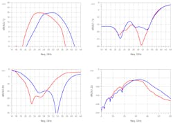
Figure 3 shows the simulated S-parameters plots of the dual-band PA. The dual-band responses are clearly evident (26-GHz band in red and 32-GHz band in blue). The amplifier shows good input and output return loss in each band and has a small signal gain of 20 dB.
The simulated large-signal performance is plotted in Fig. 4. As with the small-signal case, the performance of the amplifier operating in the 26-GHz band is plotted in red, while the 32-GHz band is shown in blue. P1dB is around 1 W (+30 dBm) for both bands, being slightly higher in the 26-GHz band and slightly lower in the 32-GHz band. The efficiency at P1dB is around 30% in the 26-GHz band, dropping to around 26% at 32 GHz.
One alternative to the dual-band approach would be to design a broadband amplifier capable of covering both bands. However, the gain, output power, and efficiency would all be lower with a broadband design. The compact layout and excellent dual-band performance demonstrated here shows the potential benefits that this approach can bring to dual-band millimeter-wave PAs. It is likely that dual-band operation will be highly desirable for 5G Ka-band systems, and this approach could bring huge benefits in terms of size and cost.
References
Devlin, Liam, “The Design of Integrated Switches and Phase Shifters,” Proceedings of the IEE Tutorial Colloquium on “Design of RFICs and MMICs,” Wednesday, November 24th, 1999, pp 2/1-14.


