Download this article as a .PDF
Large capacity is essential to the success of present and future cellular wireless networks, and a well-designed low-noise amplifier (LNA) can help increase the capacity of a small cell. A typical small cell has a range of about 10 m to 1 km compared to a traditional macrocell at a few tens of kilometers.1 As a result, a small cell can improve frequency reuse by as much as 1600×.2
On the flip side, hundreds of small cells are needed to provide the same coverage as one macrocell. Hence, it is necessary to make small cell equipment significantly less expensive than its macrocell counterpart. One way to save cost is by using one broadband radio module instead of multiple narrowband radio modules in support of different air interfaces. The LNA is an essential component for the receiver portion of a small cell’s radio module.
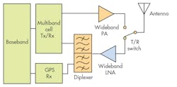
An LNA is the first stage of a radio module’s receiving section (Fig. 1). It is usually impedance matched for low noise at one frequency although, in a small wireless cell, an LNA must cover a wide range of frequencies. Resistive shunt feedback can widen an LNA’s impedance-matched bandwidth3, 4 but results in tradeoffs of noise, gain, and output-power performance5; hence, it can only be used sparingly. Fortunately, small cells have less demanding noise requirements than macrocells since they cover smaller areas.
The output-power requirements of small cells are also lower because a small cell’s low height (about 10 m) makes it less susceptible to interference.6 To compensate for the increased noise of a feedback amplifier’s configuration, a low-noise semiconductor process, such as a GaAs enhancement-mode pseudomorphic high-electron-mobility-transistor process (GaAs E-pHEMT),7, 8 can be used. Although low-noise feedback amplifiers have been realized with discrete ePHEMTs,9, 10 the use of monolithic microwave integrated circuit (MMIC) technology can significantly reduce component count by integrating amplifier, feedback network, and biasing circuits.
Such integration has been used in an SOT-363-packaged amplifier with sub-1-dB noise figure (NF) over two octaves of bandwidth.11, 12 The device’s small size and good performance have led to its adoption in many small-cell LNAs, although it is not as popular lately. While its NF performance was considered state-of-the-art when it was introduced in 2003, it has since been surpassed by competitors (Table 1).
Small cells serve a number of time-division-duplex (TDD) networks, including time-division synchronous code-division-multiple-access (TD-SCDMA) technology for Third-Generation (3G) cellular networks and time-division Long Term Evolution (TD-LTE) for Fourth-Generation (4G) cellular networks. Due to the use of a common frequency for transmit and receive functions, the LNA must be powered down during transmission to prevent overdrive. Traditionally, the power-down function is implemented off-chip by wiring a transistor switch in series with the LNA’s supply voltage. However, a competitor’s recent design integrates an LNA and power-down switch into a silicon germanium (SiGe) MMIC.13 Since this approach saves components in TDD implementations, it has been well received by carriers for use in small cells.
To improve upon this approach, it is necessary to develop a lower-cost MMIC LNA with smaller size that still provides a two-octave bandwidth. The choice of MMIC semiconductor process is critical for achieving the necessary NF performance at low cost. A 0.25-μm GaAs E-pHEMT process was selected for its excellent balance of cost and performance. Performance-wise, E-pHEMT and SiGe processes are roughly equivalent, but mask sets for E-pHEMT technology are fewer and less expensive.14, 15
Setup costs are important because of the relatively small volume requirements for small-cell LNAs compared to devices used in mass-market wireless handsets. Another factor in favor of E-pHEMT technology is the capability to integrate a switch with the amplifier.
A traditional design approach uses feedback to tune the input and output impedances to approximately the target characteristic impedance. However, at VHF and lower microwave frequencies, a large amount of feedback is required, which will significantly degrade NF and output power. Relying on feedback alone to match a GaAs E-pHEMT device resulted in a modest NF of 0.8 dB at 900 MHz.10
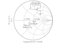
One way to reduce the feedback requirement is to tailor the gate dimensions for a good impedance match at midband frequencies. However, once the gate width has been set for a good midband match, the impedances may still vary too much over the full frequency range for realistic wideband operation. As a result, only a small amount of feedback was used to reduce the impedance spread over frequency (Fig. 2). This alternative design approach also results in less NF degradation.
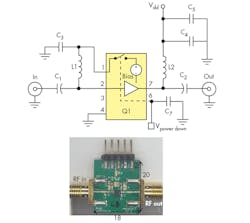
Since gain and NF are key parameters in an LNA, the E-pHEMT was configured as a common-source amplifier. Aside from the LNA, the MMIC chip also contains circuits for the power-down function, active bias, and electrostatic-discharge (ESD) protection (Fig. 3). The active bias is designed to draw a nominal 65 mA from a single +4-V dc supply.
The power-down function is performed by a switch that disconnects the E-pHEMT’s gate from the active bias. Since the function is designed to activate the LNA if its control terminal (V power-down, pin 6) is either grounded or open, the control terminal can be conveniently left unconnected in non-TDD applications.
The chip is epoxy encapsulated in an eight-lead quad-flat-no-lead (QFN) package measuring 2 × 2 × 0.75 mm3. This package was chosen for two reasons: It is 25% lower in height than the legacy device, and the absence of leads eliminates the lead-forming process.
Due to the MMIC’s high level of integration, only eight external components are needed. (Fig. 3). It is impractical to integrate these components, which perform choking and DC blocking roles, because of their large values. To create an LNA module, all of the components and connectors were assembled on a 10-mil-thick RO4350 printed-circuit board (PCB) from Rogers Corp.16 All signal and power traces are on one side of the PCB, with the ground plane on the other side. An FR-4 circuit-board backing layer was attached to the ground plane for strength and to increase the stack height of the circuit module to the standard 1.6 mm.
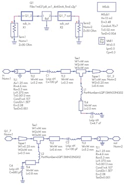
Advanced Design System 2009 (ADS 2009) simulation software from Keysight Technologies was used to simulate the LNA’s linear performance levels. The MMIC was modeled using manufacturer-supplied Touchstone-formatted file containing both S-parameters and noise parameters (Fig. 4). Inductors were modeled using manufacturer-supplied compact models.18
Other passive components (resistors and capacitors) were modeled using lumped equivalent circuit models, which only account for first-order parasitic effects. The values of the parasitic elements were estimated. Although the models were not exact, they made it possible to perform a rapid simulation of the LNA design without the need (and required resources) for performing model extractions.
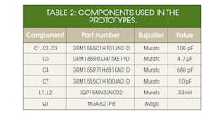
To validate the design, three experimental units were built and tested; the units were based on MMICs randomly selected from the same wafer. Other components required for the experimental units are listed in Table 2. The experimental performance shows the LNA to cover a frequency range of 0.3 to 1.6 GHz, or better than two octaves, or about a 188% fractional bandwidth. The unit is characterized by increasing noise at the lower bandedge and decreasing gain at the upper bandedge.
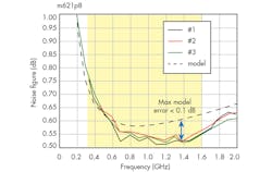
The design is capable of sub-0.8-dB NF within in its target frequency range. Variations between device samples were less than 0.05 dB. The NF of these experimental units was lowest at about 1.2 GHz, rising abruptly as frequency decreases (Fig. 5). With an NF specification set at 0.8 dB, the lowest usable frequency for the LNA is 0.3 GHz, enabling it to support T-GSM-380 (380 MHz). The simulated NF shows the same trend as the experimental results and has a maximum error of 0.1 dB over the evaluated frequency range.
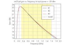
The upper end of the frequency range is 1.6 GHz due to the gain decreasing with frequency. The gain levels of the samples are highly uniform (Fig. 6). The experimental gain reaches a peak of 23 dB at about 0.3 GHz. Assuming a minimum required gain of 15 dB, then this design has an upper frequency limit of 1.6 GHz. Therefore, the highest cellular band that can be supported is LTE/WCDMA band 21 (1448 to 1463 MHz).
This frequency range also allows concurrent reception of GPS signals for base-station timing and location (Fig. 1). Within the target frequency range, the gain varies 8 dB. The simulated gain agrees with the experimental gain within a fraction of a decibel.
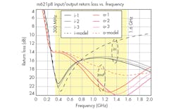
Neither input nor output matching limits the bandwidth of this design. The experimental input return loss (IRL) is better than –15 dB in the 0.3-to-1.6-GHz range. The experimental IRL varies less than 7 dB within the target frequency range (Fig. 7). Both experimental and simulated IRL minima converge at about 0.4 GHz. The simulation is relatively accurate at low frequencies but the simulation error increases at higher frequencies. Within the target frequency range, the error is less than 6 dB, probably due to the lack of precision for the models.
The experimental output return loss (ORL) is better than –14 dB in the target frequency range. The best output impedance matching occurs at about 1.4 GHz (Fig. 8). The experimental ORL variation is less than 11 dB within the target frequency range. The simulation is accurate at low frequencies, but deviates from the experimental measured results at higher frequencies—although the simulation error is less than 5 dB.
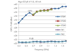
The experimental output third order intercept point (OIP3) exceeds +30 dBm within the target frequency range of 0.3 to 1.6 GHz. The OIP3 rises rapidly at low frequencies and then plateaus at higher frequencies (Fig. 8). At midband (900 MHz), the OIP3 is +36.6 dBm, which corresponds to an input IP3 of +19.6 dBm. Compared to similar devices without feedback, this OIP3 is a fraction of a decibel lower. The in-band variation in OIP3 is approximately 9 dB.
The experimental power output at 1-dB gain compression (P1dB) exceeds +20.4 dBm within the target frequency range. The P1dB is relatively flat over frequency, with an inband variation of about 0.9 dB. The corresponding input P1dB at midband (900 MHz) is +1.6 dBm. The LNA showed above-average linearity behavior. Using midband OIP3 and P1dB values, the linearity figure of merit (LFOM) was determined as equal to OIP3 – P1dB19 and equals 15.8 dB for the LNA at midband.
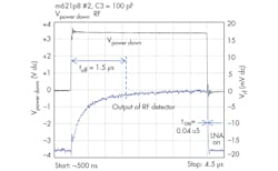
To minimize dead time in TDD applications, the integrated power-down function should ideally be capable of fast switching times. For measuring the switching speed of the integrated power-down function, the turn-on time (tON) and turn-off time (tOFF) are defined from the time at 50% of the control signal to the time at 90% of the final RF output amplitude.20 The change in the LNA’s output was observed using a negative-polarity Schottky diode detector.21 The experimental tOFF and tON times were 1.5 and 0.04 μs, respectively (Fig. 9).
The slow power-down time is due to shunt capacitor C3 lacking a discharge path. It may be possible to speed up the discharge of C3 with an external resistor, but this has not been verified. On the other hand, the tON time compares to the industry’s fastest.22 In conclusion, this MMIC implementation can provide the performances needed for small cell TDD applications with the power-down function included for reduced component count.
Acknowledgments
The author wishes to thank M.D. Suhaiza and S. Punithevati for assembling the samples, T.W. Lee and Y.Y. Liew for product design and characterization, and S.A. Asrul for supervising this work.
References
1. Anonymous, “Small Cells,” Wikipedia.
2. Anonymous, “About small cells,” (n.d.).
3. J.A. Walston and J.R. Miller, eds., “Wideband or video amplifiers,” in Transistor Circuit Design, McGraw-Hill, New York, 1963, Chap. 19.
4. B.S. Virdee, A.S. Virdee, and B.Y. Banyamin, “Broadband Feedback Amplifiers,” in Broadband Microwave Amplifiers, Artech House, Norwood, MA, 2004, section 6.5.
5. C. Baringer and C. Hull, “Amplifiers for Wireless Communications,” in RF and Microwave Circuit Design for Wireless Communications, L. E. Larson, ed., Artech House, Norwood, MA, 1997, p. 360.
6. “Outdoor LTE small cell deployment on lamp posts: A Paris city study,” Ranplan Wireless Network Design Ltd.
7. W. Wu, J.S. Wei, C. Su, R.M. Parkhurst, S.L. Fu, S. Chang, and R.B. Levitsky, “An enhancement-mode pHEMT for single-supply power amplifiers,” in Hewlett-Packard Journal, February 1998.
8. “Development of E-pHEMT Technology,” Avago white paper, June 2007.
9. A.S. Virdee and B.S. Virdee, “Computer-aided design of ultrabroadband 100 MHz to 20 GHz amplifiers,” Microwave Journal, February 2000.
10. I. Piper, “Build an E-pHEMT low-noise amplifier,” Microwaves & RF, March 2004.
11. “MGA-62563 current-adjustable low noise amplifier,” Avago data sheet, November 2004.
12. “MGA-62563 high performance GaAs MMIC amplifier,” Avago application note 5011.
13. “BGU8051,” Rev. 2, NXP product data sheet, December 2013.
14. Pat Hindle, “2010 GaAs foundry services outlook,” Microwave Journal, June 2010, pp. 20-28.
15. R.F. Kopf, A.G. Baca, and S.N.G. Chu, “Enhancement- mode power AlGasAs/InGaAs/AlGaAs,” Electrochemical Society Proceedings, Vol. 2000-1, pp. 110-118.
16. Rogers Corp., “RO4000 series high frequency circuit materials,” Rogers data sheet, Publication No. 92-004, April 2006.
17. Keysight Technologies, Advanced Design System (ADS) technical reference (Version 2009),.
18. “Library for Keysight ADS,” Murata design tools, http://www.murata.com.
19. Raymond S. Pengelly, “Improving the Linearity and Efficiency of RF Power Amplifiers,” High Frequency Electronics, September 2002, p. 26.
20. Agilent Technologies, application note, “Understanding RF/Microwave solid state switches and their applications, May 2010.
21. Agilent Technologies, datasheet 5952-8299, “423B, 8470B, 8472B, 8473B/C low barrier Schottky diode detectors,” October 2011.
22. C.L. Lim, “LNA integrates fast shutdown function,” Microwaves & RF, December 2014.
23. Guerrilla RF, GRF2104 preliminary data sheet, December 2015.

