Download this article as a .PDF
Antennas come in many shapes and sizes, although printed-circuit-board (PCB) antennas provide the capability of packing a great deal of performance into miniature footprints. Of course, many antennas—including those based on PCBs—must be designed and fabricated for minimum passive intermodulation (PIM) levels for maximum effectiveness in today’s crowded signal environments. For PCB antennas, low PIM is a function of the antenna design but also of the choice of RF/microwave circuit material, since circuit materials can contribute a great deal to the overall PIM performance of a PCB antenna.
PIM is a nonlinear, diode-like effect that results in the creation of unwanted harmonic signals when two or more signals combine (such as from different transmitters). These extra signals can cause problems when they are at sufficient energy levels and when they fall within the frequency range of a receiver and can prevent the receiver from detecting its intended in-band signals. While PIM may not impact every application, it can disrupt the operation of wireless communications systems, especially those attempting to recover low-level signals.
PIM can occur at any junction or interface with two different metals, such as connectors and cable assemblies or antennas and antenna feeds. Loose connectors and connectors with internal rust or oxidation can cause PIM. PCB materials can also be sources of PIM, whether from the materials themselves or at feed points. But by understanding how different circuit material parameters relate to PIM, it is possible to select circuit laminates that are less likely to contribute to PIM problems in PCB antennas.
PCB Antennas
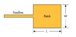
High-frequency antennas fabricated in PCB form can take on many configurations, from simple dipoles to more elaborate constructions based on ring resonators and Rotman lenses. One of the more popular PCB antennas is the microstrip patch antenna, which can be made simply and compactly for a given frequency range (Fig. 1). Many applications employ multiple patches or resonant structures on a PCB to create a beamforming network (BFN) or phased-array antenna with the capability of electronically steering the amplitude, phase, and direction of a low-profile PCB antenna structure for radar and communications systems. Compact planar PCB antennas are also of growing interest at millimeter-wave frequencies, such as for 77-GHz Advanced Driver Assistant Systems (ADAS) for automotive electronic safety systems, for such functions as blind-spot detection, automatic braking systems, and collision avoidance. Because signal power levels are low in such systems, ADAS receivers rely on high sensitivity to reliably detect radar returns reflected from targets such as pedestrians and other vehicles.
Although PIM is usually the result of inhomogenous materials in circuit junctions such as solder joints or connectors, circuit material characteristics, such as rough copper conductor surfaces and different types of plating finishes, can favor either lower or higher PIM levels. A number of circuit material parameters can be used as guidelines for achieving lower PIM in PCB antennas.
Dielectric constant (Dk) is a starting point for many engineers when selecting a circuit laminate for a design, such as a microstrip patch antenna. The effect of circuit material Dk on circuit dimensions are detailed for the four examples of the table, showing how the size of a microstrip patch antenna for a given frequency shrinks with increasing Dk value. The table was created with the help of the MWI-2017 software, which is available for free download from the Rogers Corp. website. The length (L) and width (W) of a microstrip patch antenna can be found from a pair of simple equations:
W = (c/2fr)[2/(Dkeff +1)]0.5
L = λ/[2(Dkeff)0.5] - 2ΔL
where
Dkeff = the effective dielectric constant of the microstrip circuit;
λ = the wavelength based on the microstrip circuit;
fr = the resonant frequency of the patch radiating element;
c = the speed of light in free space; and
ΔL = the extension of the patch due to electric field fringing.
A microstrip patch antenna element radiates EM energy to free space upon transmission and returns EM energy to a connected circuit (e.g., a receiver) upon reception. But the patch is just one component in a PCB antenna, with the feedline comprising another important part. The feedline transfers EM energy between the connected microstrip circuitry and the radiating patch for transmission and reception. Ideally, the patch should exhibit high radiation while a feedline should exhibit low radiation, achieving efficient transfer of energy from the circuit to the patch.
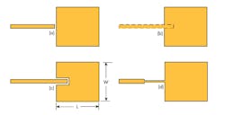
Four different feedline configurations (Fig. 2) are available for connection to a microstrip patch: loosely gap coupled, bottom layer feed (where the feedline in a multilayer circuit is beneath the patch), tightly gap coupled, and via a quarter-wavelength (λ/4) transformer. The feedlines differ in complexity and flexibility. With the bottom layer fed, for example, a designer has the option to select the best circuit material on the outer layer for optimum patch radiation and a different circuit material for the inner layers, so as to minimize radiation and insertion losses for the feedline.
Thicker circuit materials are more prone to radiation. As a result, in general, circuit materials for radiating antenna elements such as microstrip patches should be relatively thick and with low Dk value (2.2 to 3.5, for example). Circuit materials with higher Dk values can be used when it is necessary to create smaller patch antennas, although materials with higher Dk values are less prone to radiate and PCB antennas are more challenging when using circuit materials with high Dk values.
Policing PIM
Antennas guilty of high levels of PIM can cause loss of data in wireless telecommunications systems, such as 4G LTE wireless networks. Such networks rely on distributed antenna systems (DAS) for extended wireless coverage, and the same is expected to be true for emerging 5G wireless networks—albeit at higher frequencies.
For two in-band carrier signal frequencies f1 and f2 in a transceiver system, PIM can occur as mixing products of nf1 – mf2 and nf2 – mf1, where n and m are integers. The generated PIM products are categorized by order numbers, with the order determined by the sum of m and n, such as third-order PIM products of 2f1 – f2 and 2f2 – f1 (Fig. 3). Third-order products are problematic because they can fall within the receiver’s frequency band and can block reception if at suitably high levels.
The amplitudes of the PIM products is a function not only of the amplitudes of f1 and f2 but of the PIM order number, with the amplitudes of PIM products decreasing with increasing order numbers. As a result, fifth-, seventh-, and ninth-order PIM products are usually at power levels that do not affect receiver performance.
What is considered low PIM? An acceptable value varies from system to system, with −145 dBc often considered low enough for the DAS equipment used in 4G-LTE systems, which include other passive components, such as connectors and cables. In general, a level of −140 dBc or worse is considered poor PIM performance, while −150 dBc is considered good and −160 dBc is excellent.
The PIM levels of antennas and other passive components are measured in specially designed anechoic chambers in which a level as low as −170 dBc is likely beyond the ambient noise of the test chamber. A more realistic noise level for most PIM test chambers is −165 dBc when performing measurements with two +43-dBm test tones.
Low PIM is especially important when the same antenna is used for transmit and receive functions with a common feedline. Whenever transmitters and receivers are co-located in a system, any unwanted nonlinear mixing of multiple transmitted signals can result in PIM at amplitudes sufficient to degrade receiver performance. Some contributions on the part of a PCB antenna to poor PIM performance can be influenced by understanding the roles that different materials characteristics play in the generation of PIM.
The dielectric portion of a laminate, such as ceramic or PTFE material, has less impact on a laminate’s contributions to PIM than the relative surface roughness of the copper conductor layer. For circuits based on the same dielectric material (e.g., PTFE with woven-glass or ceramic filler), a circuit with rough copper conductor surface will have worse PIM performance than the same circuit with a smoother copper surface.
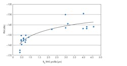
To better understand the relationship of laminate copper surface roughness to PIM, a circuit material with good PIM performance was analyzed with copper foils having much different surface roughness characteristics. The surface roughness of each copper foil was measured prior to making the circuit laminates with the foil, and the PIM performance of each of the laminates was then measured by forming a microstrip transmission-line test circuit on each laminate. The PIM was found to rise steadily with increasing copper surface roughness (Fig. 4).
The plated finish used on a PCB material can also affect the PIM performance of antennas and other passive components fabricated on the material. Ferromagnetic materials, such as nickel, are not good material ingredients for achieving low PIM levels. Studies of circuits with immersion tin as the final plated finish typically have better PIM performance than bare-copper circuits, while circuits using electroless-nickel-immersion-gold (ENIG) plated finishes provide poor PIM performance because of the nickel content.
Circuit treatments can be beneficial to achieving low PIM levels for antennas and other passive components fabricated on those treated circuits. Circuits with soldermask over bare copper typically provide better PIM performance than circuits with bare copper. Clean circuits, without residues left behind by wet chemical processing, are important foundations for low PIM performance. Circuits with any form of ionic contaminate residue can yield poor PIM performance.
Similarly, the etching quality of a circuit is also important for good PIM performance. If a conductor has been under-etched, small copper dendrites left along the edges of the circuit can cause degraded PIM performance.
The level of PIM exhibited by a passive component can be enhanced through a careful choice of circuit material, although even a low-PIM material will not cure every PIM ill for some circuits. Certain types of circuits are more susceptible to PIM than others, as an experiment with 32.7-mil-thick RO4534 circuit material from Rogers Corp. revealed. The antenna-grade laminate features a Dk of 3.4 with a tolerance of ±0.08 and low dissipation factor (low loss) of 0.0027 at 10 GHz.
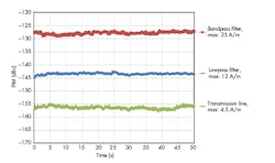
The same sheet of material was used to fabricate three different circuits: a transmission line, a bandpass filter, and a lowpass filter (Fig. 5). PIM is impacted by current density, and even though these circuits were formed on the same circuit material, the differences in PIM were significant; the filters and their higher current densities suffered much higher PIM levels than the simpler transmission-line circuit. The RO4534 material is specified for low PIM of −157 dBc when evaluated with two +43-dBm test tones using a microstrip transmission-line test vehicle.
As the experiments show, simple transmission-line circuits, as might be used for antenna feeds, can achieve close to the rated PIM levels of the material. Nontheless, PIM is also very dependent upon circuit configuration.
John Coonrod, Technical Marketing Manager
Rogers Corp., Advanced Connectivity Solutions, 100 S. Roosevelt Ave., Chandler, AZ 85226-3416; (480) 961-8398
