Download this article in PDF format.
Ultrawideband (UWB) communications technology makes use of broad expanses of frequency spectrum, transferring information at high data rates using low-energy pulses. While UWB signals are designed not to interfere with existing narrowband communications systems within the same frequency range, they are subject to interference from narrowband communications signals.
To overcome that interference problem, an UWB antenna was designed with a bandwidth of 3.1 to 11.5 GHz and with two notches; thus, the antenna doubles as a band-reject filter. The notches are designed to prevent interference from larger signals in such applications as WiMAX systems and wireless local-area networks (WLANs). The experimental antenna was fabricated on low-cost FR4 printed-circuit-board (PCB) material to demonstrate the effectiveness of the design.
A Look at UWB
Although UWB technology has existed for some time for radar applications, the Federal Communications Commission (FCC) increased interest in the frequency range from about 3.1 to 10.6 GHz for short-range, high-data-rate commercial communications.1 Many components have been designed for UWB use, including antennas based on various topologies.2-13
For UWB applications, planar antenna structures appear to offer advantages over other configurations for their simple structures, ease of fabrication, small size, low profiles, and low cost. UWB communications systems provide many benefits, such as enabling high data rates, increased security, low power consumption, and simple hardware requirements in practical applications.2 For UWB systems to be effective, however, antennas for those systems must meet several requirements, including small size; omnidirectional radiation patterns; high, stable gain across a wide frequency range; and compatibility with other required components, such as filters and amplifiers.
Of course, signals occupying the UWB frequency range must coexist with many well-established narrowband communications systems, such as IEEE 802.11a and HIPERLAN/2 WLAN systems operating in the 5- to 6-GHz range. In some European and Asian countries, WiMAX service occupies the frequency range from 3.3 to 3.6 GHz. UWB antennas have typically functioned with the addition of filters to suppress narrowband signals that might interfere with UWB operation. As an alternative approach, portions of the UWB spectrum can be notched out by developing antennas with band-notch characteristic.10-17
Building the Two-Notch Antenna
To demonstrate this design approach, an UWB antenna with two notched frequency bands was developed. Two techniques were used to achieve the notches. In one, a T-shaped slot was formed in the radiating patch on the current path of the antenna. In the other, a U-shaped parasitic strip was added above the antenna ground plane. The first notch is intended to reduce interference in the frequency band from 3.3 to 4.1 GHz. The second notch is to eliminate interference within the frequency band of 5.1 to 6.0 GHz.
CST Studio three-dimensional (3D) electronic design automation (EDA) software from Computer Simulation Technology was used in the design and simulation of the antenna.
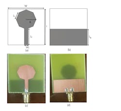
Figure 1 shows the basic antenna structure. It’s composed of an octagonal-shaped radiator with radius (r) of 8.2 mm. This radiator is interconnected with the microstrip transmission line with a line width, Wf, of 3 mm to achieve a characteristic impedance of 50 Ω; the transmission has a line length (Lf) of 13.8 mm. As may be apparent from Fig. 1b, the antenna has a partial ground plane with length (Lg) equal to 13.4 mm to achieve the desired impedance bandwidth required for UWB applications. The width (W) of the antenna is 30 mm and the length (L) is 30 mm.
1. The geometry of the dual-notch UWB antenna can be seen from these (a) front and (b) rear views of the layout as well as from (c) front and (d) rear views of the fabricated prototype.
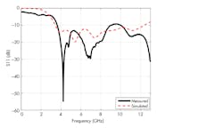
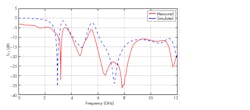
A prototype of the planar antenna was fabricated on low-cost FR4 PCB material (Figs. 1c and 1d). The FR4 circuit material exhibits relative permittivity (εr) of 4.4 and thickness of 1.6 mm. Figure 2 shows the simulated and measured return loss of the planar UWB antenna with two frequency notches. The antenna was simulated from 3.3 to 12.0 GHz with better than 10-dB return loss. From the measured results, the measured return loss is better than 10 dB from 3.3 to 10.0 GHz, showing good agreement with the simulated data.
2. The plots illustrate the two notches for the simulated and measured responses of the UWB antenna.
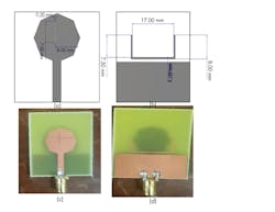
Figure 3 presents the structure of the proposed UWB antenna with the two notched frequency bands to reduce interference from other wireless applications operating within the UWB frequency range. The two notches are obtained by adding the T-shaped slot and the U-shaped parasitic strip. The T-shape slot is inserted in the radiating patch to reduce interference from WiMAX applications from 3.3 to 4 GHz, while the U- shaped parasitic strip decreases interference from WLAN applications from 5.2 to 5.9 GHz.
3. These images show similar but more detailed information than Fig. 1 for the (a) front and (b) rear views of the layout as well as from (c) front and (d) rear views of the fabricated prototype.
The length of the U-shaped parasitic strip is calculated by means of Eq. 1:
Ltotal ≈ λg/2 = c/(2fnotch(εeff)0.5 (1)
where
εeff ≈ (εr + 1)/2
and c is the speed of light in a vacuum, and εr is the relative permittivity of the PCB material.
Figures 3c, 3d, and 4 offer different views of the dual-notched-band UWB antenna prototype, which was characterized with the aid of the ZVB 20 vector network analyzer (VNA) from Rohde & Schwarz. The network analyzer is capable of high-resolution S-parameter measurements to 20 GHz. Figure 4 shows measurements made with the VNA, along with simulated return loss for the proposed UWB antenna with dual notched bands.
4. More detailed than Fig. 2, these plots depict the two notches in the response of the UWB antenna.
The Verdict
Examining the simulated results, the antenna operates from 3 to 12 GHz with return loss of better than 10 dB except from 3.3 to 4.0 GHz, which is a notch intended to suppress signals from WiMAX applications, and from 5.2 to 6.0 GHz, which is a notch aimed at WLAN applications, where the return loss is about 3 dB. From the measurements, it’s apparent that the return loss is better than 10 dB from 3.2 GHz to about 12 GHz except for the two notched frequency bands. The measurements show good agreement with the simulated performance plots.
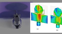
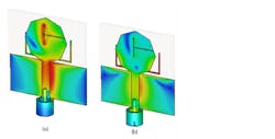
However, there are some discrepancies between the simulated results and the measured performance of the prototype, resulting from losses due to soldering and the antenna fabrication process. The simulated current flow is primarily concentrated around the T-shaped slot at 3.6 GHz (Fig. 5a), which is the center frequency of the notch intended to reduce interference from WiMAX applications.
5. The simulated current distributions for the antenna are shown at 3.6 and 5.5 GHz.
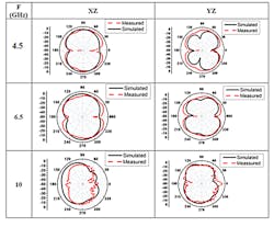
It’s also apparent that current flow is concentrated around the U-shaped parasitic strip at 5.5 GHz (Fig. 5b), which is the center frequency of the notch intended to reduce interference from WLAN applications. The radiation patterns of the UWB antenna prototype was measured while inside an anechoic chamber, at 4.5, 6.7, and 10.0 GHz for the main planes—the x-z and y-z radiation planes.
6. The measured and simulated radiation patterns for the UWB were plotted at 4.5, 6.5, and 10.0 GHz.
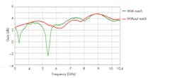
Figure 6 shows the simulated and measured radiation patterns at those three test frequencies, revealing that the antenna exhibits an omnidirectional radiation pattern in the y-z plane and a bidirectional radiation pattern in the x-z plane. As the plots in Fig. 6 show, there’s reasonable agreement between the simulated and measured results for the radiation patterns of the UWB antenna. Figure 7 compares the simulated gain of the antenna, with and without the two notches. The average gain without the notches is about 3 dB. The simulated gains for the lower- and higher-frequency notches is about −2 and −1 dB, respectively.
7. These traces show the simulated peak gain of the antenna, with and without the two notches.
In short, as the measurements on the prototype reveal, this UWB planar antenna with two built-in notches is promising as a means of simplifying UWB communications systems design, as it eliminates the need for at least two of those additional filters. The UWB antenna can be fabricated on low-cost circuit-board material with good performance. It operates from 3.1 to 12.0 GHz with a compact footprint and, without additional hardware, can suppress interference occurring in the frequency bands of 3.3 to 3.9 GHz and 5.2 to 5.9 GHz.
References
1. Federal Communications Commission, First Report and Order, Revision of Part 15 of the Commission’s Rules Regarding Ultrawideband Transmission Systems, February 2002.
2. R. Zhang, G. Fu, Z.-Y. Zhang, and Q.-X. Wang, “A wideband planar dipole antenna with parasitic patches,” Progress in Electromagnetics Research Letters, Vol. 20, 2011, pp. 137-145.
3. Ahmed A. Ibrahim, F. Hesham F. A. Hamed, Mohammed Alla ElDin, Azhar Abdel-alla, and Eman Yahia, “A compact Planar UWB Antenna with Band-Notched Characteristics,” ICET, 2014, pp. 1-4.
4. J. Yang and A. Kishk, “The Self-Grounded Bow-Tie Antenna,” IEEE International Symposium on Antennas and Propagation, August 2011, pp. 1452-1455.
5. M. M. S. Taheri, H. R. Hassani, and S. M. A. Nezhad, “UWB Printed Slot Antenna with Bluetooth and Dual Notch Bands,” IEEE Antennas & Wireless Propagation Letters, Vol. 10, 2011, pp. 255-258.
6. Ali Wael and Ahmed A. Ibrahim, “A Compact Double-Sided MIMO Antenna with Improved Isolation for UWB Applications,” International Journal of Electronics and Communications, Vol. 82, 2017.
7. Ahmed A. Ibrahim, Mahmoud A. Abdalla, and Zhirun Hu, “Design of A Compact MIMO Antenna with Asymmetric Coplanar Strip-Fed for UWB Applications,” Microwave and Optical Technology Letters, Vol. 59, No. 1, 2017.
8. K. S. Sultan, H. A. Mohamed, and M. M. Eltayeb “Low SAR, Novel compact Textile Wearable Antenna for Body Communications” 3rd International Conference on New Paradigms in Electronics & Information Technology (PEIT'015), Egypt, November 2015, pp. 1-4.
9. Ahmed A Ibrahim, Mahmoud A. Abdalla, and Ahmed Boutejdar, “Hybrid Technique Delivers Dual-Notch UWB Antenna,” Microwaves & RF, Vol. 55, No. 4, April 2016, pp. 56-60.
10. Wael Ali, Ahmed A. Ibrahim, and Jan Machac, “Compact Size UWB Monopole Antenna with Triple Band-Notches,” Radio Engineering Journal, Vol. 26, No. 1, 2017.
11. Ahmed A. Ibrahim, Wael Ali, and Jan Machac, “UWB Monopole Antenna with Band Notched Characteristics Mitigating Interference with WiMAX,” Radio Engineering Journal, Vol. 26, No. 2, 2017.
12. X. J. Liao, H.-C. Yang, and L. Y. Yang, “Aperture UWB Antenna with Triple Band-Notched Characteristics,” Electronics Letters, Vol. 44, No. 12, 2011, pp. 77–79.
13. Ahmed A. Ibrahim, Jan Machac, and Raed M. Shubair, “Compact UWB MIMO Antenna with Pattern Diversity and Band Rejection Characteristics,” Microwave and Optical Technology Letters, Vol. 59, No. 6, 2017.
14. K. G. Thomas, and M. Sreenivasan, “A simple ultrawideband planar rectangular printed antenna with band dispensation,” IEEE Transactions on Antennas and Propagation, Vol. 58, No. 1, 2010, pp. 27–34.
15. A. M. Abbosh, and M. E. Bialkowski, “Design of UWB Planar Band-Notched Antenna using Parasitic Elements,” IEEE Transactions on Antennas & Propagation, Vol. 57, No. 3, 2009, pp. 796-799.
16. A. Boutejdar, A. A. Ibrahim, and E. P. Burte, “Novel Microstrip Antenna Aims at UWB Applications,” Microwaves & RF, Vol. 54, No. X, 2015, pp. xx-xx.
17. A. A. Ibrahim, M. A Abdalla, and A. Boutejdar, “Resonator switching techniques for notched UWB antenna in wireless applications,” IET Microwaves, Antennas & Propagation, Vol. 9, No. 13, 1468–1477, 2015.
