Doherty PAs Go Broadband Using Impedance Adjustment Network
Download this article in PDF format.
Changzhong Chen of Shaanxi Aircraft Industry (Group) Co., Ltd. is also a co-author.
Skyrocketing demand for high data throughput in modern wireless communication systems is leading to the use of high peak-to-average-power-ratio (PAPR) signals. This situation poses a challenge to RF power-amplifier (PA) designs for future mobile communication systems. The Doherty PA (DPA) has been widely adopted in base-station infrastructure due to its excellent ability to maintain high efficiency over an extended power range.1 As a result, DPA bandwidth has become a research hotspot.
In recent years, many efforts have taken place to expand the bandwidth of the DPA. Ref. 2 presents a new configuration for designing broadband DPAs that involves employing a post-matching network and low-order impedance inverters. Furthermore, a novel combiner represents a non-negligible method for implementing broadband DPAs.3, 4 In Ref. 3, it was shown that adding a shunt LC tank at the drain of the peaking transistor improved the DPA’s bandwidth.
Similarly, in Ref. 4, the LC was replaced with a shunt short-circuited quarter-wavelength line to form a new combined network. The novel broadband DPA based on the continuous-mode technique was proposed in Ref. 5, which focused on manipulating harmonic components in a DPA structure to achieve improved bandwidth and efficiency.
From a theoretical point of view, it’s important that the output impedance of the peaking PA is infinite, which holds true in the references mentioned. However, it’s difficult for the offset line to provide large output impedances for a broadband design. A broadband continuous-mode DPA that was realized through the non-infinite output impedances of the peaking stage broke the previous assumption of peaking output impedances.6
After analyzing the influence of the peaking output impedances of the DPA in wideband operation, this article proposes a novel output impedance adjustment topology of the peaking stage for the DPA. A high-impedance, π-type transmission-line network replaces part of the offset line of the peaking PA to adjust the output impedance value and distribution range, improving the DPA performance at the output power back-off (OPBO) level. At the same time, the impedance-matching requirement is still satisfied.
Proposed DPA Architecture
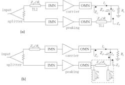
1. Shown are simplified schematic diagrams of a conventional DPA (a) and the proposed DPA (b).
Figure 1a shows the structure of a conventional DPA. The carrier amplifier operates in Class-AB mode, while the peaking amplifier is biased in Class-C mode. IC and IP are the output currents of the carrier and peaking branches, respectively. Based on active-load modulation, IP = γIC at saturation and IP = 0 at OPBO, which means the corresponding modulated impedances of carrier and peaking stages, ZC and ZP, at OPBO and saturation (Sat) are:RL is the load of the DPA, which is considered to be 25 Ω in this design. The characteristic impedance and electrical length of TL1 are (1 + 1/γ)RL and θ1, respectively. TL1 is tuned so that the output impedance of the peaking PA is infinite. TL2 with an electrical length of θ2 balances the phase difference between the carrier and peaking branches.
It’s assumed that the peaking stage has no effect on the carrier PA due to the off-state ideally being at the OPBO level. However, it’s difficult to guarantee that the output impedance of the peaking PA (ZP−out) will be infinite across a wide bandwidth. We specify the ZP−out as:
Normally, the real part of ZP−out is too small to be ignored. In Ref. 7, theoretical analysis demonstrates that DPAs require different output impedances of the peaking stage to attain superior performance at different normalized frequencies. However, there’s limited bandwidth (50%) to obtain the maximum output power at the corresponding normalized frequency.
In fact, as the |XPO| becomes smaller as the normalized frequency moves further away from the center frequency in a wider bandwidth range, more power leakage is produced at OPBO. That, in turn, degrades the 6-dB back-off drain efficiency until the point of ineffectiveness is reached. This is an important factor that limits the bandwidth of the DPA.
Thus, it’s necessary to make the output impedances as close to infinite as possible to reduce the impact on the carrier PA in the broadband range. It also means that the distribution range of the output impedances of the peaking PA is minimized with the center frequency located at infinity, which must be compromised with the pursuit of maximum output power.
A novel output impedance adjustment topology of the peaking PA is therefore proposed (Fig. 1b) along with the simplified schematic diagram of the entire DPA. Specifically, a high-impedance π-type network replaces part of the output phase-shift line of the peaking PA found in a conventional DPA structure. The middle high-impedance transmission line is used to reduce the distribution range of output impedances over frequency. The open transmission lines play a role in adjusting the output matching network. It’s verified by simulation that the output impedance matching effect of the peaking PA is acceptable.
This structure is simple and does not add difficulty to the DPA design. Here, the characteristic impedance ZA in the proposed network is 85 Ω. The electrical lengths, θA and θB, are adjusted according to the output matching network (OMN) and the design frequency band. In this design, θA and θB are 12.5° and 22°, respectively.
To achieve the desired behavior in the proposed design, the OMN of the peaking amplifier must be properly designed. For the frequency range of 1.5 to 2.7 GHz, the range of the optimal load impedances at the device package plane of the amplifier can be obtained via load-pull simulations.
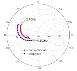
Fully considering the influence of peaking matching impedances on power and efficiency, a broadband OMN of the peaking PA was designed. This broadband OMN also acts as the peaking OMN of the conventional DPA. The simulated peaking matching impedances of the conventional DPA are plotted in Figure 2. An offset line should be added to the peaking inverter, providing large output impedances for a broadband design. γ = 1 is determined simply. Obviously, the characteristic impedance of the offset line is suggested to be set as 2RL.
2. The Smith chart plots the simulated peaking matching impedances of the conventional DPA and proposed DPA.
After completing the design of the entire conventional DPA, the proposed DPA was obtained by replacing part of the offset line of the peaking stage with the high-impedance π-type network mentioned. The length of the phase compensation line can be adjusted if necessary. The rest of the DPA remains intact.
As noted, Figure 2 plotted the simulated peaking matching impedances of the proposed DPA. A simple conclusion, as can be drawn from the simulation experience, is that the distribution range of output impedances of the peaking stage is smaller when the trajectory of peaking matching impedances is closer to the left edge of the Smith chart. It’s also verified by comparing the two tracks in Figures 2 and 3.
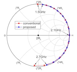
3. Here, the distribution of the output impedances of the conventional peaking PA and the proposed peaking PA is shown across the entire band of interest.
To verify the distribution change of the peaking output impedances and facilitate comparison, Figure 3 indicates that the output impedance regions of the conventional peaking PA and proposed peaking PA across the entire band of interest are distributed clockwise on the edge of the Smith chart along with the increase in frequency when the center frequency is at infinity. The reference impedance of the Smith chart is set to 2RL.
A comparison of the two impedance lines reveals that the new structure reduces the variation range of the off-state output impedances. On the other hand, this also means that DPAs can be designed over a wider frequency range due to reducing the restriction of peaking output impedance.
One area of concern is how the changes in peaking matching impedances will impact DPA bandwidth and performance. Fortunately, by comparing the performance of the two DPAs described, one can see that the output power and efficiency of the proposed DPA are improved at the upper and lower frequency points of the target bandwidth. That is, under the same index, the proposed DPA can be obtained with a wider bandwidth. The method described in this article does not affect the initial DPA design—and it’s convenient to implement.
Simulation and Measurement
For verification, the DPA prototype was implemented using two CGH40010F 10-W gallium-nitride (GaN) high-electron-mobility transistors (HEMTs) from Wolfspeed within the targeted frequency band of 1.5 to 2.7 GHz. Taconic’s RF-35 substrate used in this design had a dielectric constant of 3.5, a conductor thickness of 35 μm, and a substrate thickness of 0.76 mm. A 3-dB Wilkinson power divider was employed to evenly split the input power.
For Class-AB operation, the bias conditions of the carrier amplifier were VGC = −2.8 V and VDDC = +28 V. For Class-C operation of the peaking amplifier, the bias conditions were VGP = −5.6 V and VDDP = +30 V.
The input matching networks were designed by using the stepped-impedance matching network to cover the required bandwidth. Figure 4 shows the microstrip dimensions of the output matching circuits. Simulations were performed using Keysight’s Advanced Design System (ADS) with the device model provided by the vendor. The carrier output matching network was designed with consideration of both the saturation and low-power region. To realize the impedance matching from 50 to 25 Ω in the target band, a fourth-order stepped-impedance matching network was used as the post-matching network.
4. These are the output matching circuits of the proposed DPA.
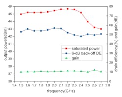
Figure 5 reveals the simulated performances of the broadband DPA. It’s clear that the 6-dB back-off drain efficiency is better than 48.1%, while the saturated output power is greater than +43 dBm. Furthermore, the gain is greater than 10 dB.
5. Plotted are the simulated saturated power levels, 6-dB back-off drain efficiencies, and gain.
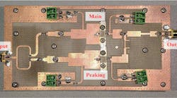
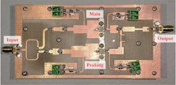
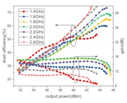
Figure 6 shows a photograph of the final PA. To assess the performance of the fabricated DPA, gain and efficiency versus output power at different frequencies were measured under continuous-wave (CW) operation (Fig. 7).
6. This is a photograph of the fabricated DPA.
7. The measured drain efficiencies and gain of the fabricated DPA versus output power are revealed at various frequencies.
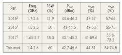
Due to fabrication errors and the inaccurate capacitor and transistor models, the measurement results have a slight frequency offset in comparison to the simulation design. The measured drain efficiencies from 1.4 to 2.6 GHz are better than 44% and 54% at 6-dB OPBO and the maximum power levels, respectively. The saturated power is greater than +42.7 dBm with a peak of +45.6 dBm. In addition, greater than 8.6 dB of gain is achieved. The table compares the performance of this proposed DPA and the other broadband DPA.
This is a comparison between various references and the work presented in this article.
Conclusion
A DPA topology with a novel output impedance adjustment network of the peaking stage is proposed in this article. This development can enhance performance by reducing the distribution range of the output impedances of the peaking stage in a broadband scenario. A DPA based on the proposed configuration was fabricated. An overall fractional bandwidth of 60% (1.4 to 2.6 GHz) was achieved with a drain efficiency greater than 44% at 6-dB back-off power.
Acknowledgments
This work was supported by China Scholarship Council (20163192) and the National Natural Science Foundation of China (61001012).
Qinghua Tang, Xiaoyu Zhang, and Lamin Zhan are from the School of Optical and Electronic Information, Huazhong University of Science and Technology, Wuhan 430074, People’s Republic of China
Baoquan Hu and Changzhong Chen are from Shaanxi Aircraft Industry (Group) Co., Ltd., Hanzhong Shanxi, China
References
1. Cripps, S. C.: RF power amplifiers for wireless communications, Artech House, Norwood, MA, 2006, 2nd ed.
2. Pang, J., He, S., Huang, C., Dai, Z., Peng, J., and You, F.: “A post-matching Doherty power amplifier employing low-order impedance inverters for broadband applications,” IEEE Microw. Theory Tech., 2015, 63, (12), pp. 4061-4071, doi: 10.1109/TMTT.2015.2495201.
3. Abadi, M. N. A., Golestaneh, H., Sarbishaei, H., and Boumaiza, S.: “An extended bandwidth Doherty power amplifier using a novel output combiner,” IEEE MTT-S Int. Dig., Tampa, FL, June 2014, pp. 1-4., doi: 10.1109/MWSYM.2014.6848510.
4. Chen, S., Wang, G., Cheng, Z., and Xue, Q.: “A bandwidth enhanced Doherty power amplifier with a compact output combiner,” IEEE Microw. Wirel. Compon. Lett., 2016, 26, (6), pp. 434-436, doi: 10.1109/LMWC.2016.2558108.
5. Chen, X., Chen, W., Ghannouchi, F. M., Feng, Z., and Liu, Y.: “A broadband Doherty power amplifier based on continuous-mode technology,” IEEE Trans. Microw. Theory Tech., 2016, 64, (12), pp. 4505-4517, doi: 10.1109/TMTT.2016.2623705.
6. Shi, W., He, S., Zhu, X., Song, B., Zhu, Z., Naah, G., and Zhang, M.: “Broadband continuous-mode Doherty power amplifiers with noninfinity peaking impedance,” IEEE Trans. Microw. Theory Tech., 2018, 66, (2), pp. 1034-1046, doi: 10.1109/TMTT.2017.2749224.
7. Shi, W., He, S., You, F., Xie, H., Naah, G., Liu, Q. A., and Li, Q.: “The influence of the output impedances of peaking power amplifier on broadband Doherty amplifiers,” IEEE Trans. Microw. Theory Tech., 2017, 65, (8), pp. 3002-3013, doi: 10.1109/TMTT.2017.2673822.
